Switching device and storage unit, and memory system

a technology of switching device and storage unit, which is applied in the direction of digital storage, semiconductor devices, instruments, etc., can solve the problems of large floor area per unit cell of resistive memory using access transistor, and it is not easy to increase the capacity of resistive memory, so as to achieve larger capacity, the floor area per unit cell is made smaller, and the capacity is increased.

Inactive Publication Date: 2021-02-04
SONY SEMICON SOLUTIONS CORP
View PDF1 Cites 1 Cited by
  • Summary
  • Abstract
  • Description
  • Claims
  • Application Information

AI Technical Summary

Benefits of technology

[0067]In recent years, a larger capacity has been demanded of a non-volatile memory, and various resistive memories have been discussed. However, in a 1T1R configuration in which one memory device is disposed for one access transistor, the area per unit cell is larger, and thus it has a limitation in achieving the larger capacity. Accordingly, a cross-point memory having a three-dimensional structure has been considered.
[0068]In the cross-point memory, as described above, memory cells each including a memory device and a switching device that are coupled in series are disposed at points of intersection (cross-points) between intersecting wiring lines, and thus the floor area per unit cell is made smaller. For example, it is possible to achieve an area per unit cell of 2F2, where F denotes a reference line width. Therefore, it is possible to make the cell area smaller, and by stacking a plurality of cross-point arrays in layers, it becomes possible to achieve a larger-capacity memory. Examples of the switching device include a PN diode, an avalanche diode, and a switching device including metallic oxide. Besides these, a switching device including, for example, a chalcogenide material (an ovonic threshold switch (OTS) device) may be used.
[0069]To suppress leakage current in the cross-point array, the switching device used in the cross-point memory is demanded to be low in leakage current when it is off and have less variation in switching threshold voltage. To address this, for example, there is disclosed a method of using carbon in an electrode material in contact with a chalcogenide layer included in a switching device, and it is reported that for example, in a case where the chalcogenide layer includes selenium (Se), variation in threshold voltage is improved by using a carbon material in an electrode. However, the above-described switching device is disadvantageous in that it is difficult to maintain the characteristics at a process temperature (for example, 400° C.).
[0070]A heat-resisting property is able to be enhanced, for example, by adding an element such as germanium (Ge) or arsenic (As) to the chalcogenide layer, thereby changing the composition ratio; however, it leads to an issue that variation in switching threshold voltage becomes larger. Furthermore, for example, in a case where tellurium (Te) is used in the chalcogenide layer, and Ge is added to that chalcogenide layer, variation in switching threshold voltage is improved; however, if an added amount of Ge is too much, there is an issue that the switching threshold voltage decreases, and the leakage current increases. In this way, despite using the carbon material in the electrode, it is still difficult to reduce variation in switching threshold voltage while reducing generation of leakage current.
[0071]In contrast, in the present embodiment, as the lower electrode 21 and the upper electrode 23 that hold the switching layer 22 including at least one chalcogen element selected from sulfur (S), selenium (Se), and tellurium (Te) between them, the carbon-containing layers 21B and 23B including carbon (C) and, as an additive element, at least one of germanium (Ge), phosphorus (P), or arsenic (As) are provided. Thus, the above-described additive element is diffused in the vicinity of the interface with the switching layer 22, and it becomes possible to form an excellent contact interface with the switching layer 22.
[0072]From the above, in the switching device 20 of the present embodiment, as the lower electrode 21 and the upper electrode 23 that hold the switching layer 22 between them, the carbon-containing layers 21B and 23B including carbon (C) and, as an additive element, at least one of germanium (Ge), phosphorus (P), or arsenic (As) are formed. Thus, the additive element is diffused in the vicinity of the interface with the switching layer 22, and an excellent contact interface is formed between the carbon-containing layers 21B and 23B and the switching layer 22. Therefore, it is possible to reduce generation of leakage current and variation in switching threshold voltage. Accordingly, it becomes possible to reduce the occurrence of an operating error of a large-scale cross-point memory cell array, and thus becomes possible to provide a larger-capacity cross-point memory.

Problems solved by technology

However, the existing resistive memory using an access transistor is large in floor area per unit cell.
Therefore, as compared with, for example, a NAND flash memory or the like, it is not easy to increase the capacity of the resistive memory even if it is scaled down by using the same design rule.

Method used


Image

  • Switching device and storage unit, and memory system
  • Switching device and storage unit, and memory system
  • Switching device and storage unit, and memory system

Examples


embodiment

1. Embodiment

1-1. Configuration of Switching Device

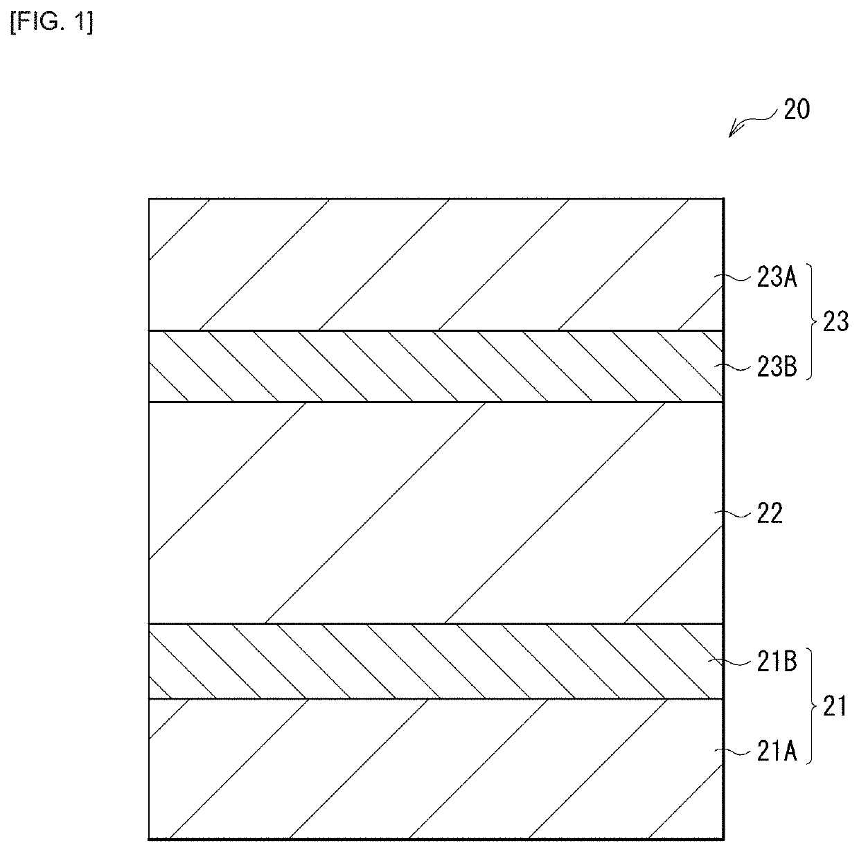
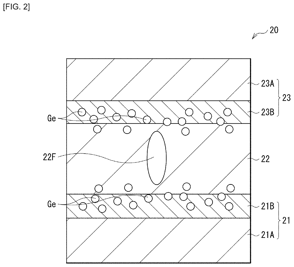
[0033]FIG. 1 illustrates an example of a cross-sectional configuration of a switching device (a switching device 20) according to an embodiment of the present disclosure. This switching device 20 is for selectively activating, for example, of a plurality of storage devices provided in a memory cell array 1 having a so-called cross-point array structure illustrated in FIG. 3, any one (a memory device 30; FIG. 3) of the plurality of storage devices. The switching device 20 is coupled in series to the memory device 30 (specifically, a memory layer 31), and includes a lower electrode 21 (a first electrode), a switching layer 22, and an upper electrode 23 (a second electrode) in this order. The switching device 20 of the present embodiment has a configuration in which the lower electrode 21 and the upper electrode 23 are configured as a stack of a metal layer 21A or 23A and a carbon-containing layer 21B or 23B; the carbon-containing laye...

modification examples

2. Modification Examples

2-1. Modification Example 1

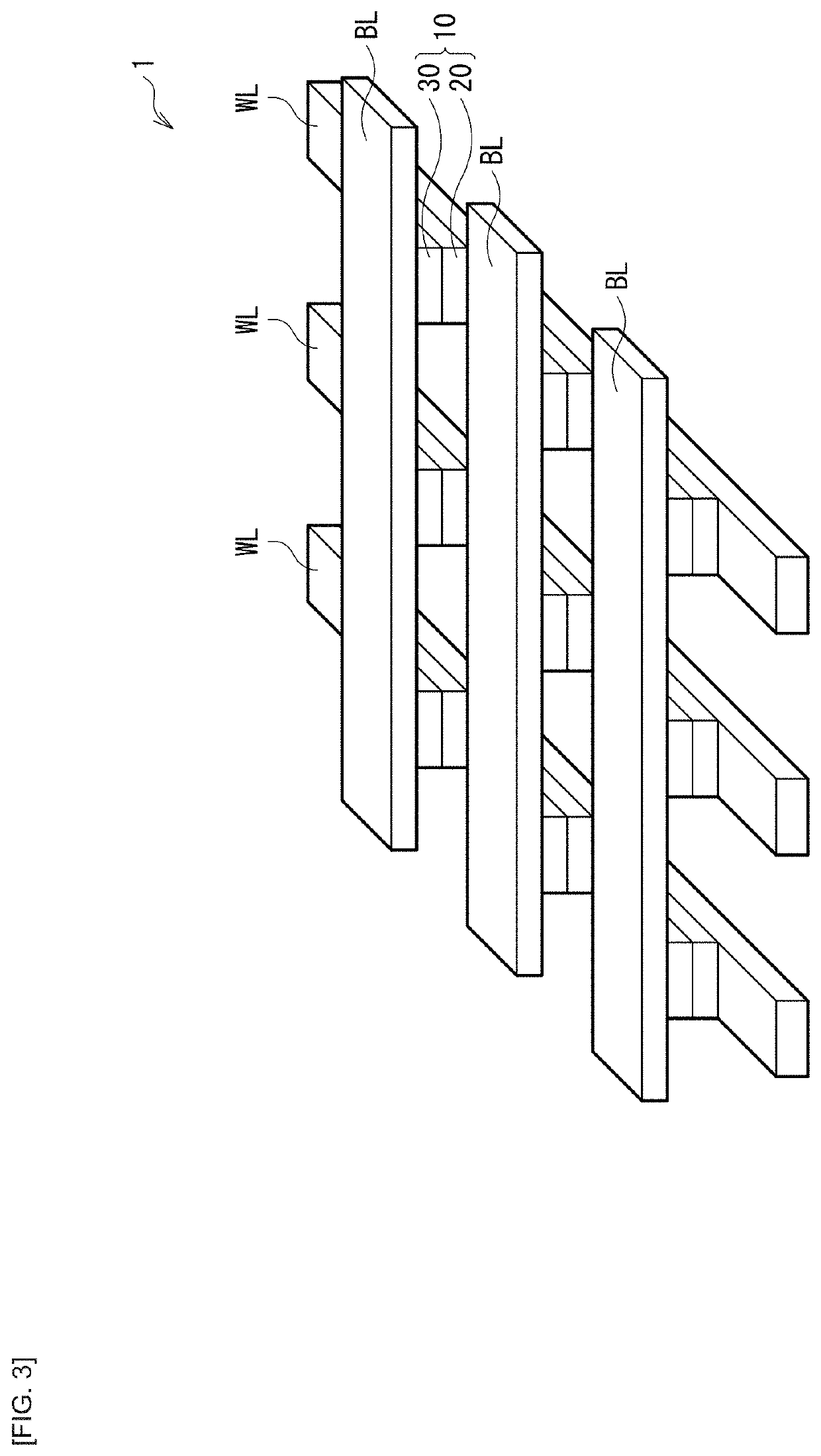
[0075]FIG. 7 is a perspective view of an example of a configuration of a memory cell array 2 according to a modification example of the present disclosure. This memory cell array 2 has a so-called cross-point array structure as with the above-described memory cell array 1. In the present modification example, the respective memory layers 31 of the memory devices 30 extend along the bit lines BL extending in the same direction. The respective switching layers 22 of the switching devices 20 extend along the word lines WL extending in a direction different from the extending direction of the bit lines BL (for example, a direction orthogonal to the extending direction of the bit lines BL). At each of cross-points between the plurality of word lines WL and the plurality of bit lines BL, the switching layer 22 and the memory layer 31 are stacked through the intermediate electrode 41.

[0076]In this way, the switching devices 20 and the memo...

modification example 2

2-2. Modification Example 2

[0077]FIGS. 8 to 11 are perspective views of examples of respective configurations of memory cell arrays 3 to 6 having a three-dimensional structure according to modification examples of the present disclosure. In these memory cell arrays having a three-dimensional structure, the word lines WL extend in the same direction. The bit lines BL extend in the same direction that is a direction different from the extending direction of the word lines WL (for example, a direction orthogonal to the extending direction of the word lines WL). Furthermore, the plurality of word lines WL and the plurality of bit lines BL are each disposed in multiple layers.

[0078]In a case where the plurality of word lines WL is disposed to be divided into multiple layers, the plurality of bit lines BL is disposed in a layer between a first layer in which multiple word lines WL are disposed and a second layer that is adjacent to the first layer and multiple word lines WL are disposed t...


PUM

PropertyMeasurementUnit
thicknessaaaaaaaaaa
thicknessaaaaaaaaaa
thicknessaaaaaaaaaa

Abstract

A switching device according to an embodiment of the present disclosure includes: a first electrode; a second electrode disposed to be opposed to the first electrode; and a switching layer provided between the first electrode and the second electrode. The switching layer includes at least one chalcogen element selected from sulfur (S), selenium (Se), and tellurium (Te). At least one of the first electrode or the second electrode includes carbon (C) and, as an additive element, at least one of germanium (Ge), phosphorus (P), or arsenic (As).

Description

TECHNICAL FIELD[0001]The present disclosure relates to a switching device having a chalcogenide layer between electrodes and a storage unit including the switching device, and a memory system.BACKGROUND ART[0002]In recent years, a larger capacity has been demanded of a non-volatile memory for data storage typified by a resistive memory, such as a ReRAM (Resistance Random Access Memory) or a PRAM (Phase-Change Random Access Memory) (registered trademark). However, the existing resistive memory using an access transistor is large in floor area per unit cell. Therefore, as compared with, for example, a NAND flash memory or the like, it is not easy to increase the capacity of the resistive memory even if it is scaled down by using the same design rule. Meanwhile, in a case of using a so-called cross-point array structure in which memory devices are disposed at points of intersection (cross-points) between intersecting wiring lines, the floor area per unit cell is smaller, and thus it be...

Claims


Application Information

Patent Timeline
Patent Type & Authority Applications(United States)
IPC IPC(8): H01L45/00H01L27/24
CPCH01L45/1253H01L27/24H01L45/065H01L45/141H01L27/105G11C13/0004H10B63/24H10B61/10H10B63/84H10B63/80H10N70/245H10N70/24H10N70/8416H10N70/20H10N70/883H10N70/231H10N70/826H10B99/00H10B63/00H10N70/841H10N70/235H10N70/882
Inventor OHBA, KAZUHIROSEI, HIROAKIYASUDA, SHUICHIRO
Owner SONY SEMICON SOLUTIONS CORP
Why Eureka
Try Eureka