

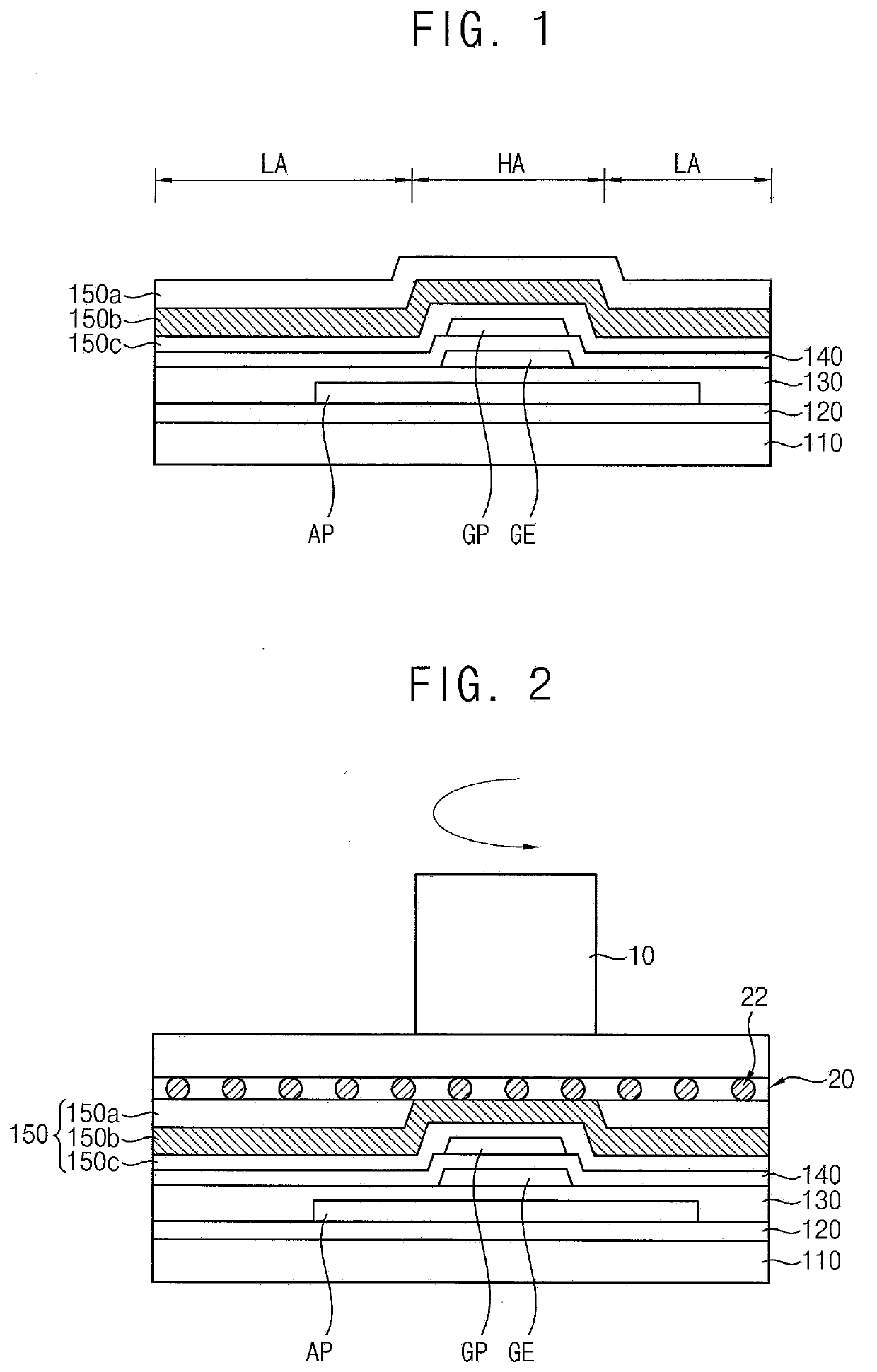
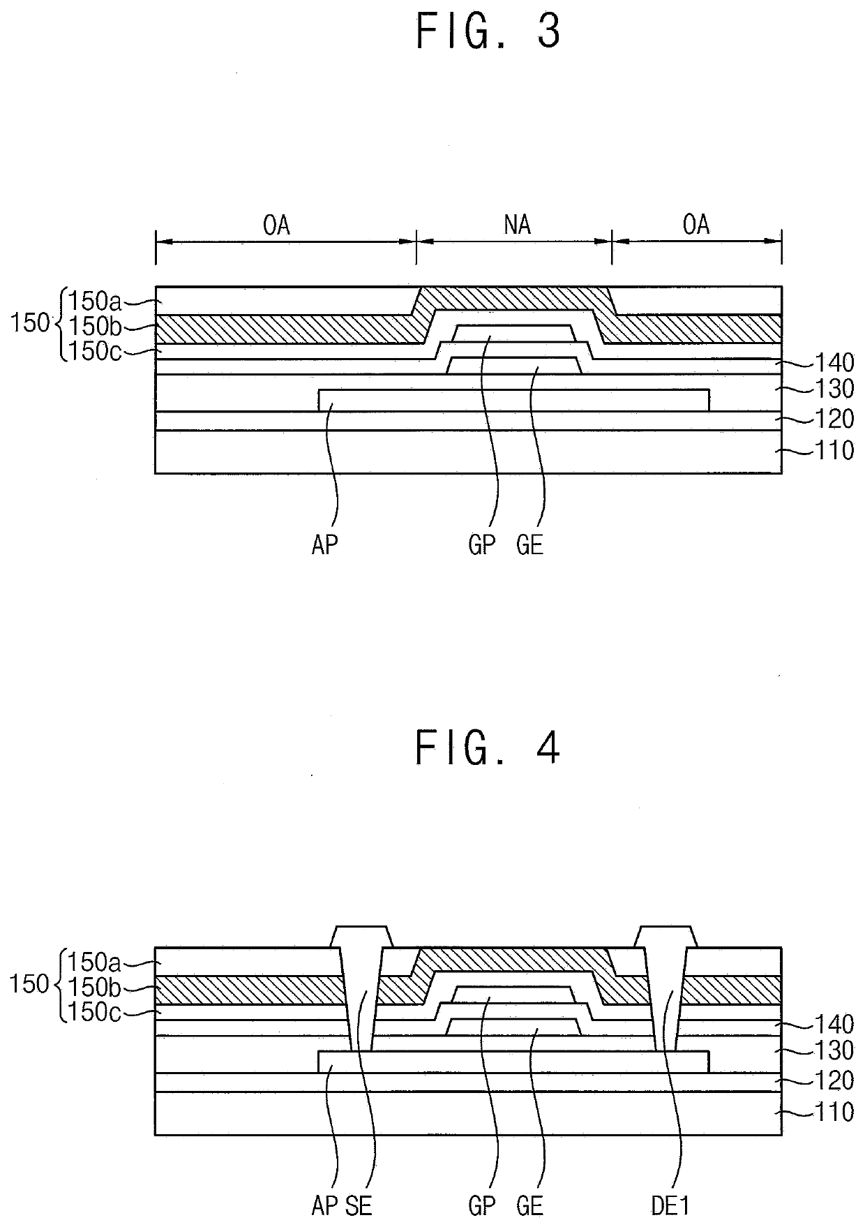
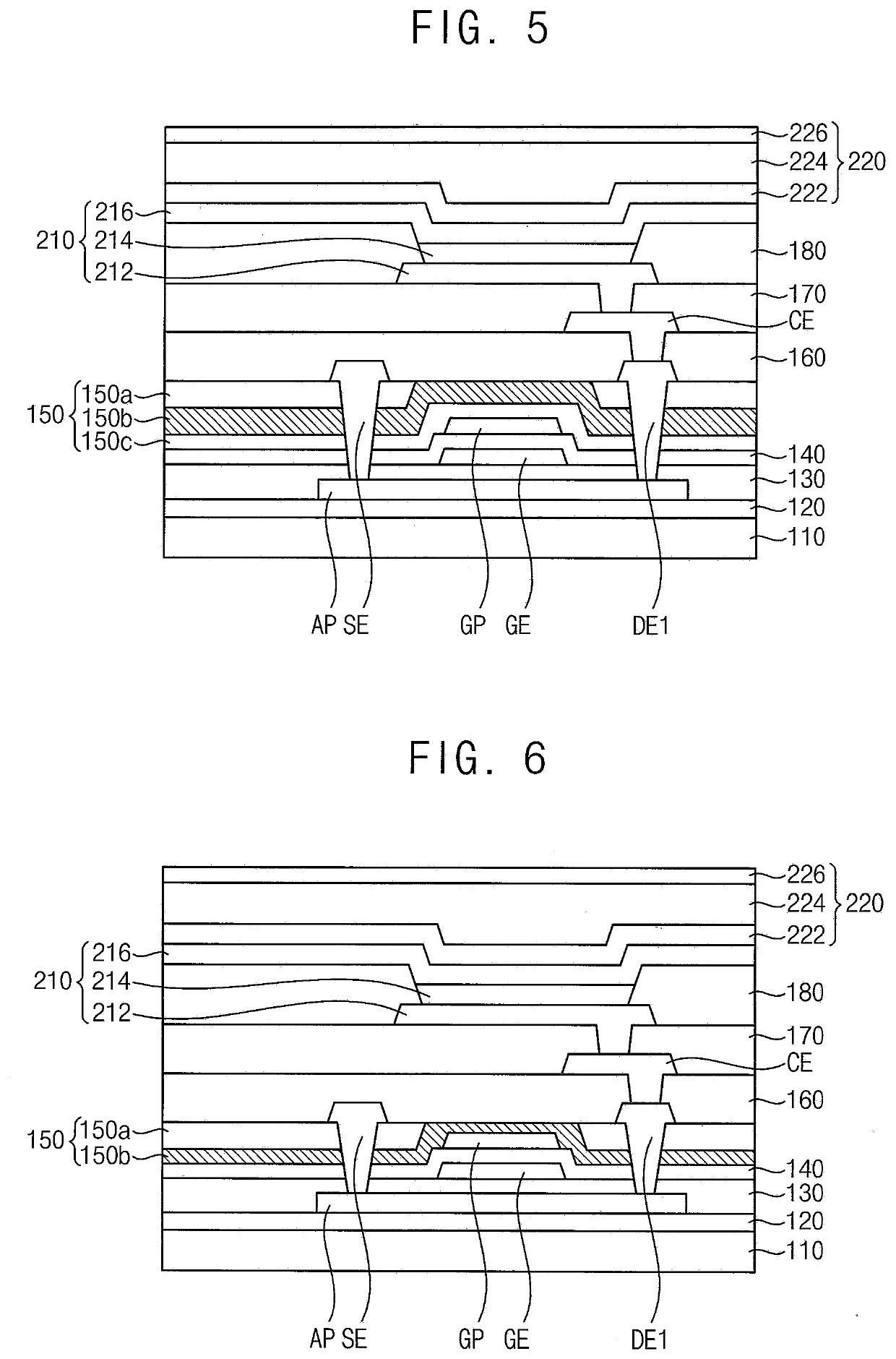
Polishing slurry, method for manufacturing a display device using the same and display device
a technology of display device and slurry, which is applied in the direction of semiconductor devices, other chemical processes, chemistry apparatus and processes, etc., can solve the problems of disconnection or undesired increase of skew, and achieve the effect of increasing the uniformity of the profile of a pattern formed on the planarized insulation layer, small residual distribution ratio, and large selectivity
- Summary
- Abstract
- Description
- Claims
- Application Information
AI Technical Summary
Benefits of technology
Problems solved by technology
Method used
Image

Examples
experiment 1
f an Effect Depending on a Content of an Oxide-Polishing Promoter
[0122]Samples of polishing slurries including 1 wt % of wet ceria particles, 0.02 wt % of a polyethylene oxide / polypropylene oxide copolymer as a dispersing agent, 0 wt % to 0.1 wt % of picolinic acid as an oxide-polishing promoter and a remainder of deionized water were prepared, and sodium hydroxide was added thereto such that the pH was about 4. A polishing rate of each samples for an SiO2 layer and Si3N4 layer was measured under the following conditions and represented by the following Table 1.
[0123][Experimental Conditions 1]
[0124]Polishing apparatus: G&P Poli-300
[0125]Polishing pad: Suba-400
[0126]Polishing speed (head / table): 80 / 80 rpm
[0127]Wafer pressure: 4 psi
[0128]Sample size: 4×4 cm2
[0129]Polishing time: 1 minute
TABLE 1SamplePicolinicPolishing rate (Å / min)PolishingnumberacidSiO2 layerSi3N4 layerselectivity1 0 wt %114128 1:120.01 wt %230125 2:130.02 wt %66899 7:140.03 wt %8717811:150.04 wt %9127113:160.05 wt...
experiment 2
f an Effect Depending on a Content of a Nitride-Polishing Inhibitor
[0131]Samples of polishing slurries including 1 wt % of wet ceria particles, 0.02 wt % of a polyethylene oxide / polypropylene oxide copolymer as a dispersing agent, 0.04 wt % of picolinic acid as an oxide-polishing promoter, 0 wt % to 0.1 wt % of glutamic acid as a nitride-polishing inhibitor and a remainder of deionized water were prepared, and sodium hydroxide was added thereto such that the pH was about 4. A polishing rate of each samples for an SiO2 layer an Si3N4 layer was measured under the same conditions as Experiment 1 and represented by the following Table 2.
TABLE 2SampleGlutamicPolishing rate (Å / min)PolishingnumberacidSiO2 layerSi3N4 layerselectivity1 0 wt %9127113:120.01 wt %9156614:130.02 wt %9246115:140.03 wt %9594322:150.04 wt %9712049:160.05 wt %10041191:170.06 wt %9981283:180.07 wt %9401278:190.08 wt %9111370:1100.09 wt %8141174:111 0.1 wt %6851069:1
[0132]Referring to Table 2, when the content of the...
experiment 3
f an Effect on a Large-Sized Substrate
[0133]Samples of polishing slurries including 1 wt % of wet ceria particles, 0.02 wt % of a polyethylene oxide / polypropylene oxide copolymer as a dispersing agent, 0.04 wt % of picolinic acid as an oxide-polishing promoter, 0.05 wt % of glutamic acid as a nitride-polishing inhibitor and a remainder of deionized water were prepared, and sodium hydroxide was added thereto such that the pH was about 4. A polishing rate of each samples for an SiO2 layer an Si3N4 layer was measured under the following conditions and represented by the following Table 3.
[0134][Experimental Conditions 2]
[0135]Polishing apparatus: CMT CLCD-800
[0136]Polishing pad: Suba-400
[0137]Polishing speed (table): 1) 50 rpm 2) 70 rpm
[0138]Wafer pressure: 1 psi
[0139]Sample size: 2G glass (370×470 mm2)
[0140]Polishing time: 1 minute
TABLE 3SamplePolishing speedPolishing rate (Å / min)Polishingnumber(table)SiO2 layerSi3N4 layerselectivity150 rpm9707.5129:1270 rpm13488169:1
[0141]Referring t...
PUM
| Property | Measurement | Unit |
|---|---|---|
| diameter | aaaaa | aaaaa |
| diameter | aaaaa | aaaaa |
| wt % | aaaaa | aaaaa |
Abstract
Description
Claims
Application Information