

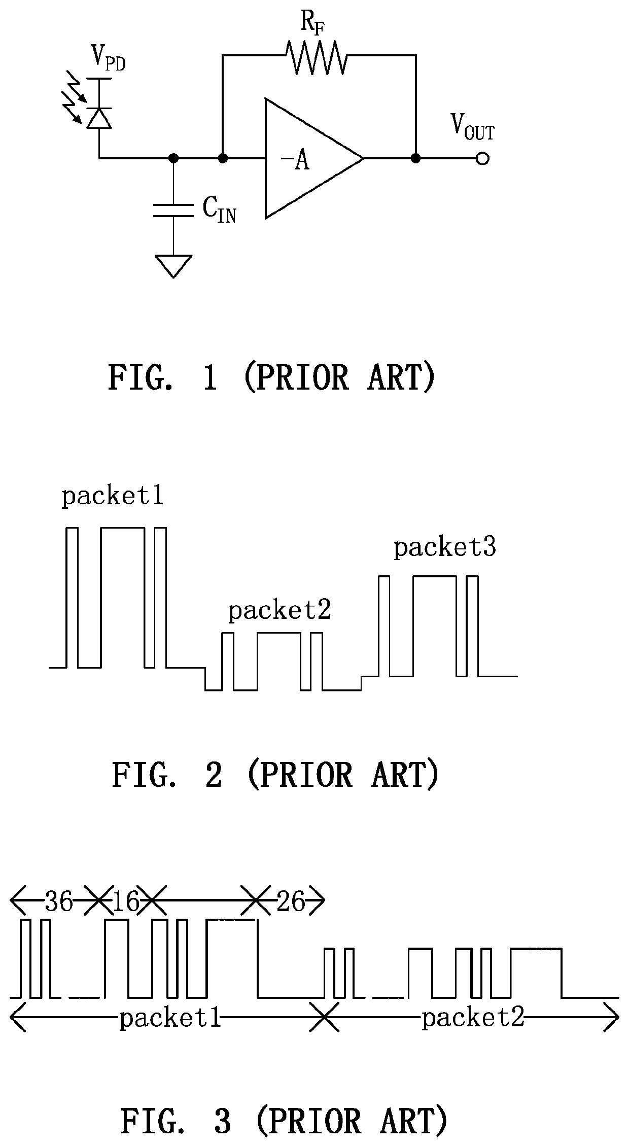
Automatic gain control method and circuit for use in burst-mode transimpedance amplifier
- Summary
- Abstract
- Description
- Claims
- Application Information
AI Technical Summary
Benefits of technology
Problems solved by technology
Method used
Image

Examples
embodiment 1
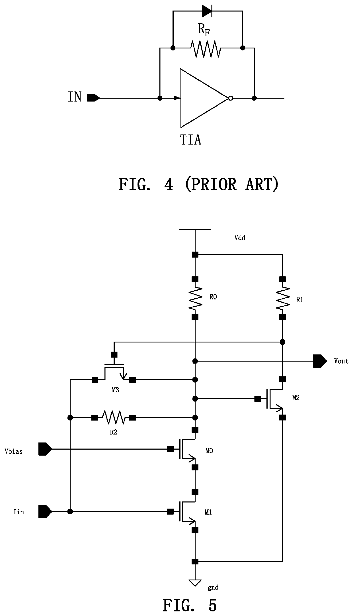
[0040]Referring to FIG. 5, an automatic gain control circuit for a burst-mode transimpedance amplifier comprises a transimpedance amplifier, a common-source amplifier, and an NMOS transistor M3.
[0041]The transimpedance amplifier includes a feedback resistor R2 and a cascode. The cascode includes an NMOS transistor M1, an NMOS transistor M0, and a resistor R0. Wherein, a gate of the NMOS transistor M1 serves as an input terminal Iin of the transimpedance amplifier. A gate of the NMOS transistor M0 is connected to a bias voltage Vbia. A drain of the NMOS transistor M1 is connected to a source of the NMOS transistor M0. A source of the NMOS transistor M1 is grounded. The feedback resistor R2 is connected between the gate of the NMOS transistor M1 and a drain of the NMOS transistor M0. The resistor R0 is connected between the drain of the NMOS transistor M0 and a power supply voltage Vdd. As a simple replacement of this embodiment, the cascode may use other structures, which does not af...
embodiment 2
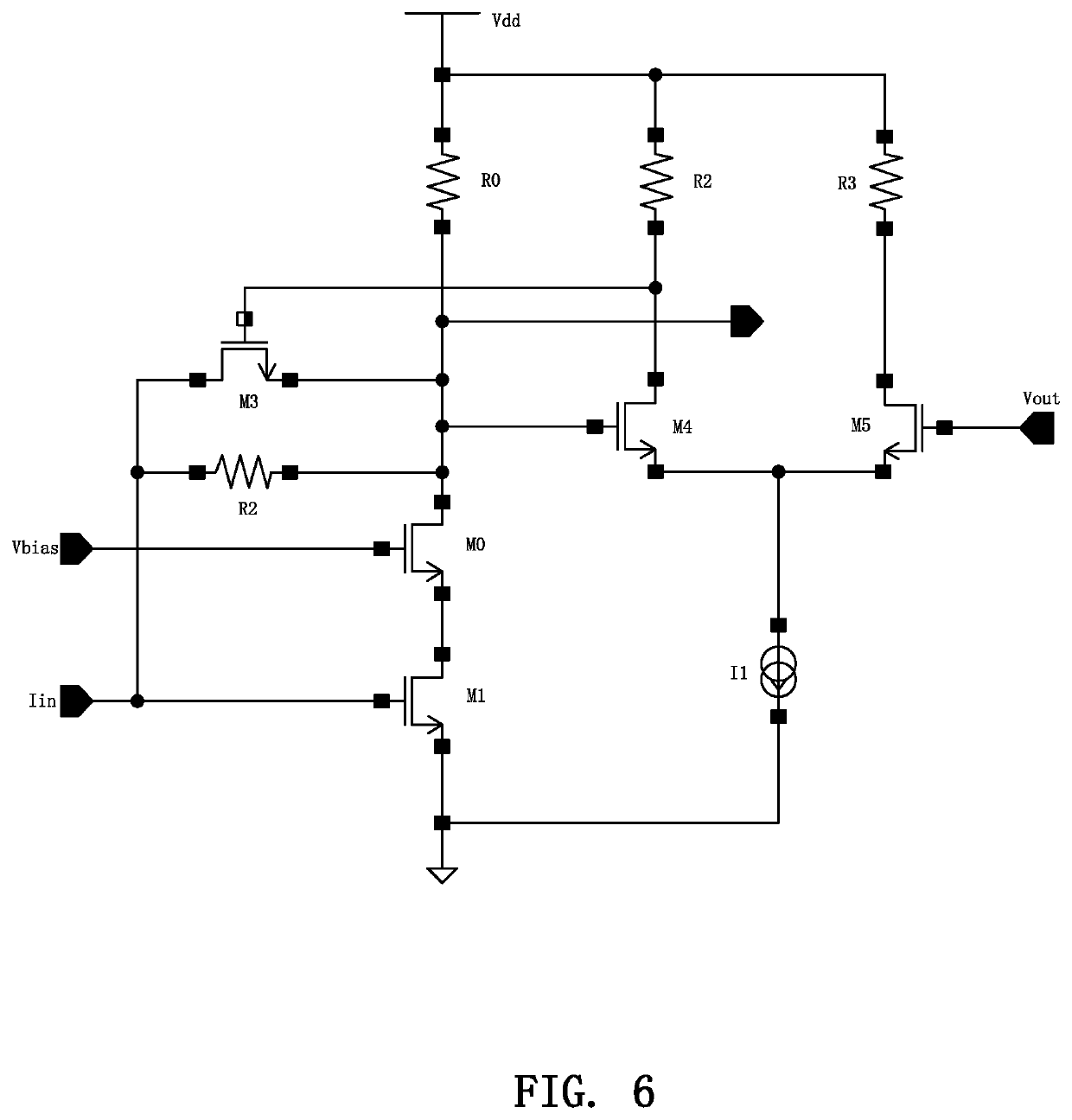
[0045]The difference between the second embodiment and the first embodiment is that in the second embodiment, the common-source amplifier is a common-source differential amplifier, including an NOMS transistor M4, an NMOS transistor M5, a resistor R2, a resistor R3, and a constant current source I1.
[0046]Wherein, a gate of the NOMS transistor M4 serves as an input terminal of the common-source differential amplifier. A gate of the NOMS transistor M5 is biased at a fixed reference voltage Vref. A drain of the NOMS transistor M4 serves as an output terminal of the common-source differential amplifier.
[0047]The resistors R2 and R3 are connected between the drains of the NOMS transistor M4 and the NMOS transistor M5 and the power supply voltage Vdd, respectively. Sources of the NOMS transistor M4 and the NMOS transistor M5 are connected and grounded through the current source I1.
[0048]When the input current of the transimpedance amplifier is zero, by properly setting the parameters of e...
PUM
 Abstract
Description
Claims
Application Information