Silicon Controlled Rectifier and Method for Making the Same

a technology of silicon controlled rectifiers and rectifiers, applied in the field of semiconductor devices, can solve the problems of low-voltage pmos devices, difficult to be implemented in practice, easy to catch-up effects, etc., and achieve the effect of increasing manufacturing complexity and saving layout area

Active Publication Date: 2021-10-28
SHANGHAI HUALI MICROELECTRONICS CORP
View PDF4 Cites 0 Cited by
  • Summary
  • Abstract
  • Description
  • Claims
  • Application Information

AI Technical Summary

Benefits of technology

[0041]In the silicon controlled rectifier provided in an aspect of the present application, the trigger voltage of the no-snapback silicon controlled rectifier can be increased within a specific range by increasing a reverse breakdown voltage of a parasitic PN diode that determines the trigger voltage, facilitating the reduction in the number of series stages required by application of multi-stage series connection to high-voltage electro-static discharge protection, and thereby achieving the object of saving the layout area. The method for manufacturing a silicon controlled rectifier provided in another aspect of the present application is compatible with an existing CMOS process, and can manufacture a no-snapback silicon controlled rectifier having a trigger voltage that can be further increased, without increasing the manufacturing complexity.

Problems solved by technology

The electro-static discharge protection design of a high-voltage circuit is always a technical problem, because unlike an ordinary low-voltage device, a high-voltage device (such as an LDMOS), which is the core of the high-voltage circuit, is inapplicable to the electro-static discharge protection design due to very poor characteristics presented by a snapback curve of the high-voltage device, which are reflected in the following two points: 1. a holding voltage (Vh) is excessively low, usually greatly lower than an operating voltage of the high-voltage circuit, so a latch-up effect is easy to occur during normal operation of the high-voltage circuit; and 2. a secondary breakdown current (thermal breakdown current, It2) is excessively low, resulting from localized current crowding occurring when the LDMOS discharges an ESD current due to the structural characteristics of the device.
Therefore, the following two ideas are usually adopted to achieve the electro-static discharge protection design of the high-voltage circuit in the industry: 1. the structure of the high-voltage device used in an electro-static discharge protection module is adjusted to optimize the snapback curve, so that the high-voltage device is applicable to the electro-static discharge protection design, and the adjustment, however, is difficult to be implemented in practice because of the structural characteristics of the high-voltage device; and 2. a specific number of low-voltage electro-static discharge protection devices are connected in series to form an electro-static discharge protection circuit that can hold a high voltage.
However, the defect of the low-voltage PMOS devices lies in a relatively small secondary breakdown current (It2) of the snapback, so the industry continuously performs researches to develop a no-snapback electro-static discharge protection device having a relatively high secondary breakdown current.
However, the defect of the novel no-snapback silicon controlled rectifier lies in a relatively large device size, in particular a relatively large layout area in multi-stage series connection.

Method used


Image

  • Silicon Controlled Rectifier and Method for Making the Same
  • Silicon Controlled Rectifier and Method for Making the Same
  • Silicon Controlled Rectifier and Method for Making the Same

Examples


Embodiment Construction

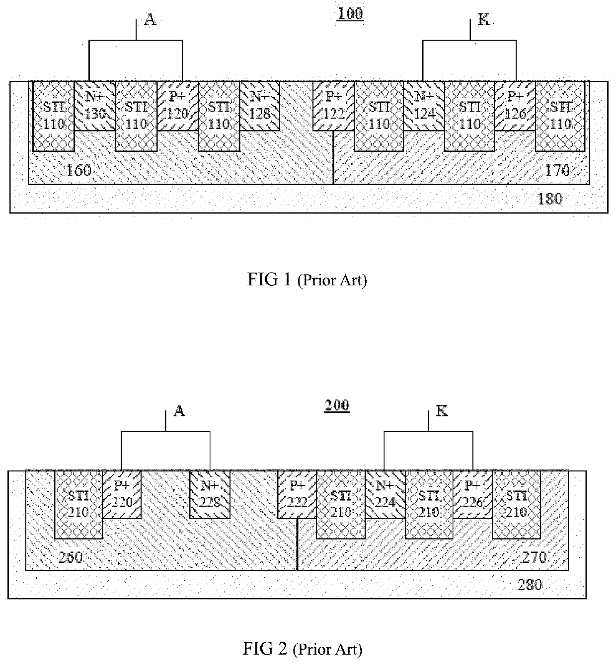
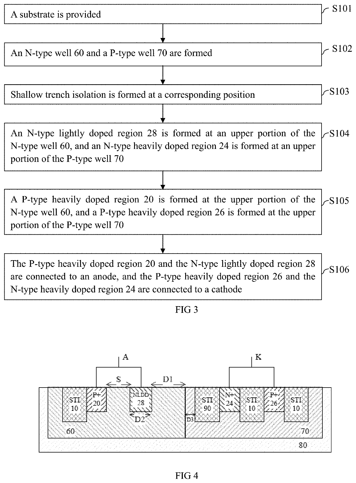
[0069]In order to further increase a trigger voltage of a no-snapback silicon controlled rectifier, the present application provides a silicon controlled rectifier structure and a manufacturing method thereof. The present application further provides other embodiments.

[0070]The following description is provided to enable a person skilled in the art to implement and use the present application and apply it into specific application scenarios. Various modifications and various uses in different applications will obvious to a person skilled in the art, and the general principle defined herein can be applied to embodiments in a relatively wide range. Therefore, the present application is not limited to the embodiments given herein, but should be granted the broadest scope consistent with the principle and novel feature disclosed herein.

[0071]In the following detailed description, many specific details are set forth to provide a more thorough understanding of the present application. How...


PUM

PropertyMeasurementUnit
width D1aaaaaaaaaa
width D3aaaaaaaaaa
widthaaaaaaaaaa

Abstract

The application provides a SCR and a manufacturing method thereof. The SCR comprises: a P-type heavily doped region 20 and an N-type lightly doped region 28 forming an anode formed on the upper part of an N-type well 60, a P-type heavily doped region 26 and an N-type heavily doped region 24 forming a cathode formed on the upper part of a P-type well 70, an active region of the N-type well 60 is between the N-type lightly doped region 28 and an interface of the N-type well 60 and the P-type well 70, a STI is provided between the N-type heavily doped region 24 and the interface, the STI is adjacent to the N-type heavily doped region 24, and an active region of the P-type well 70 is provided between the STI and the interface. The present application can improve trigger voltage of the SCR and save layout area.

Description

CROSS-REFERENCES TO RELATED APPLICATIONS[0001]This application claims priority to Chinese Patent Application No. 202010350852.9 filed on Apr. 28, 2020, the disclosure of which is incorporated herein by reference in its entirety.TECHNICAL FIELD[0002]The present application relates to the field of semiconductors, in particular to a no-snapback silicon controlled rectifier structure and a manufacturing method thereof.BACKGROUND[0003]The electro-static discharge protection design of a high-voltage circuit is always a technical problem, because unlike an ordinary low-voltage device, a high-voltage device (such as an LDMOS), which is the core of the high-voltage circuit, is inapplicable to the electro-static discharge protection design due to very poor characteristics presented by a snapback curve of the high-voltage device, which are reflected in the following two points: 1. a holding voltage (Vh) is excessively low, usually greatly lower than an operating voltage of the high-voltage cir...

Claims


Application Information

Patent Timeline
Patent Type & Authority Applications(United States)
IPC IPC(8): H01L27/02H01L21/8228
CPCH01L27/0262H01L21/8228H01L29/87H01L29/861H01L29/0649
Inventor ZHU, TIANZHIHUANG, GUANQUNCHEN, HAOYUSHAO, HUA
Owner SHANGHAI HUALI MICROELECTRONICS CORP
Why Eureka
Try Eureka