Thin film transistor, manufacturing method thereof, and display panel

Active Publication Date: 2021-12-02
SHENZHEN CHINA STAR OPTOELECTRONICS SEMICON DISPLAY TECH CO LTD
View PDF0 Cites 0 Cited by
  • Summary
  • Abstract
  • Description
  • Claims
  • Application Information

AI Technical Summary

Benefits of technology

[0081]The present disclosure can effectively increase an electron concentration in the active layer and improve a mobility of the thin film transistor by setting number of the indium oxidation layers in a stacked structure of the active layer in the thin film transistor to at least two. At the same time, the active layer adopts the stacked structure of a N-layer ind

Problems solved by technology

However, current top-gate IGZO TFTs cannot balance both high mobility and high uniformity, res

Method used


Image

  • Thin film transistor, manufacturing method thereof, and display panel
  • Thin film transistor, manufacturing method thereof, and display panel
  • Thin film transistor, manufacturing method thereof, and display panel

Examples


Example

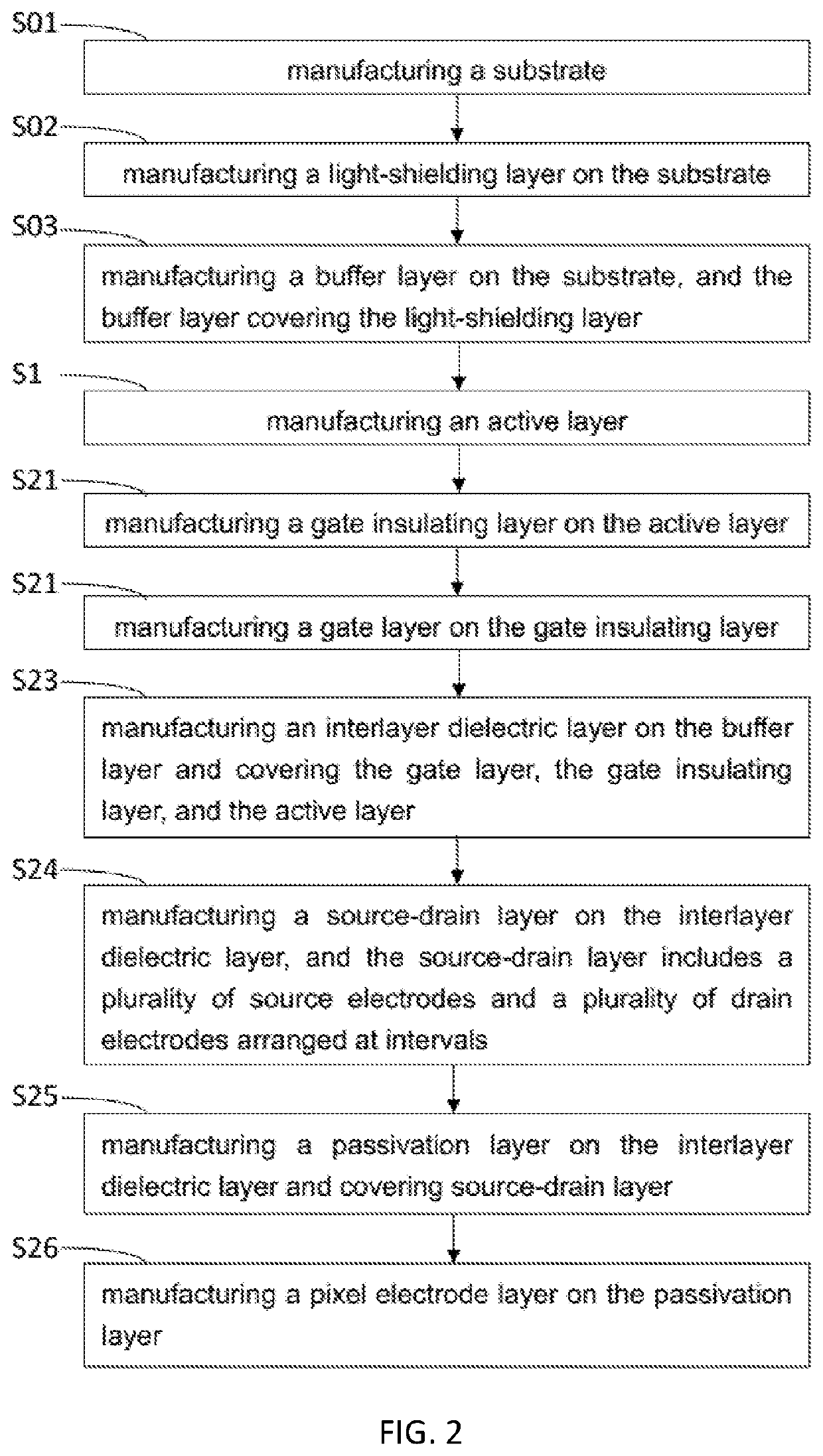
[0092]To make the objectives, technical solutions, and effects of the present disclosure clearer and more specific, the present disclosure will be described in further detail below with reference to the accompanying figures and embodiments. It should be understood that the specific embodiments described herein are only used to explain the present disclosure and are not intended to limit the present disclosure.

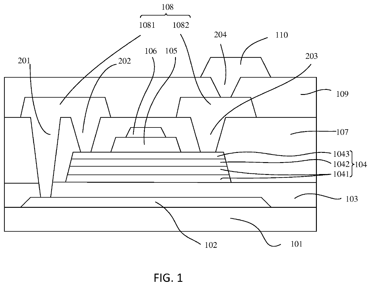
[0093]As shown in FIG. 1, one embodiment of the present disclosure provides a thin film transistor. The thin film transistor includes an active layer 104. The active layer 104 includes a plurality of stacked structures, and each of the stacked structures includes: an N-layer indium oxidation (InOx) layer 1041, a gallium oxidation (GaOx) layer 1042, and a zinc oxidation (ZnOx) layer 1043, where N is an integer greater than 1. The gallium oxidation layer 1042 is disposed on the N-layer indium oxidation layer 1041. The zinc oxidation layer 1043 is disposed on the gallium oxidation...


PUM


Abstract

A thin film transistor is provided. The thin film transistor includes an active layer, and the active layer includes a plurality of stacked structures, and each of the stacked structures includes: a N-layer indium oxidation layer; a gallium oxidation layer, the gallium oxidation layer is provided on the indium oxidation layer of the N-layer indium oxidation layer; and a zinc oxidation layer is provided on the gallium oxidation layer. These stacked structures improve the performance of the thin film transistor. A preparation method of the thin film transistor and a display panel containing the thin film transistor is also provided.

Description

FIELD OF INVENTION[0001]The present disclosure relates to the field of display technology, and more particularly, to a thin film transistor and manufacturing method thereof, and a display panel.BACKGROUND OF INVENTION[0002]Recently, metal oxide thin film transistors (TFTs) have been widely used in active matrix liquid crystal display (AMLCD) devices and active-matrix organic light-emitting diode (AMOLED) display devices. AMLCD devices and AMOLED display devices that have adopted metal oxide TFTs have significant advantages such as high resolution, large size, high refresh frequency, and high transmittance across the spectrum of visible light, which have wide application prospects in the field of display.[0003]Indium gallium zinc oxide (IGZO) TFTs are a representative oxide TFT, which has a variety of typical structures. Among them, top-gate IGZO TFTs have been widely used because of advantages such as a small parasitic capacitance, lower mask usage during a manufacturing process, an...

Claims


Application Information

Patent Timeline
IPC IPC(8): H01L29/786H01L27/32G02F1/1368H01L27/12G02F1/1362
CPCH01L29/78684H01L29/7869H01L27/3272G02F1/1368G02F1/136209H01L29/78633H01L27/1259H01L27/1248H01L27/1225H01L29/78648H10K59/126
Inventor LUO, CHUANBAO
Owner SHENZHEN CHINA STAR OPTOELECTRONICS SEMICON DISPLAY TECH CO LTD
Why Eureka
Try Eureka