
Electrical component

a technology of electrical components and components, applied in the field of electrical components, can solve the problems of unrecoverable failure of electrical components, degradation of piezoelectric and electrical properties of materials, and ceramic materials that are not good conductors of electricity

Pending Publication Date: 2022-01-06
XAAR TECH LTD
View PDF0 Cites 0 Cited by
  • Summary
  • Abstract
  • Description
  • Claims
  • Application Information

AI Technical Summary

Benefits of technology

This patent is about a way to protect electrical elements from damage caused by chemicals. It uses a special layer made of insulation material that is applied to the electrical elements. This layer helps to prevent failures in the electrical components and increases the reliability and yield of the manufacturing process. This technique can be used in various applications such as inkjet printing or 3D printing.

Problems solved by technology

One challenge of providing a reliable electrical element is to ensure proper passivation between the electrodes of individual electrical elements, protection of the individual piezoelectric members and insulation of an electrical component, as a whole, from the external environment especially humidity and chemicals that may cause short circuits and / or corrosion and / or degradation of the electrical component which may, eventually, lead to unrecoverable failure of the electrical component.
The ceramic material typically is not a good conductor of electricity.
The piezoelectric members themselves are susceptible to chemical attack that can lead to a degradation of the piezoelectric and electrical properties of the material.
Moreover, etch-damaged piezoelectric members may be particularly vulnerable and offer paths for a chemical attack to diffuse further internally in the piezoelectric member.
Meanwhile, thinner passivation layers may not provide adequate protection.
As is well known to the skilled person, commonly used methods of deposition of passivation coatings very rarely produce defect-free layers.
Once again, thicker layers may be characterised by a lower density of defects with respect to thinner layers but they have a negative impact on the displacement of the electrical element.
Furthermore there may be humidity and / or harmful chemicals present in the external environment during manufacture and / or during operation.
Unpredictable imperfections may be present in the bonding, for example a layer of bonding material, between the capping layer and the electric component where the one or more electrical elements are formed.
Such defects may cause leaks of chemicals through the capping layer and towards the one or more electrical elements.
The problem of leaks through the bonding of the capping layer may be exacerbated by the presence of randomly distributed defects in the form of pinholes or micro-cracks in the passivation structure.
Those defects may be difficult to avoid, as well as to identify and mend and they constitute weakness spots that may provide paths for chemicals to find their way to the one or more electrical elements.
The contact of chemicals with the electrical features of the one or more electrical elements, may cause corrosion, shorts and, eventually, fatal failure of one or more electrical elements.
Failure of one electrical element, in an arrangement of electrical elements incorporated within the same electrical component, may lead to complete component failure, even when a continuous layer of passivation overlies the failed electrical element and the neighbouring electrical elements.
However, alumina may be particularly susceptible to chemical attack, for example, in some environments, such as aqueous environments, and / or as a result of moisture / chemicals ingress from the external environment which may be due to non-ideal bonding of the capping layer.
However, this compensation to retain device functionality has historically not been possible where continuous passivation layers with a high susceptibility to chemical attack are used.
This weakness may then be compounded where non-ideal bonding is present at the capping layer, which increases the likelihood of chemical attack from the external environment.

Method used


Image

  • Electrical component
  • Electrical component
  • Electrical component

Examples


Embodiment Construction

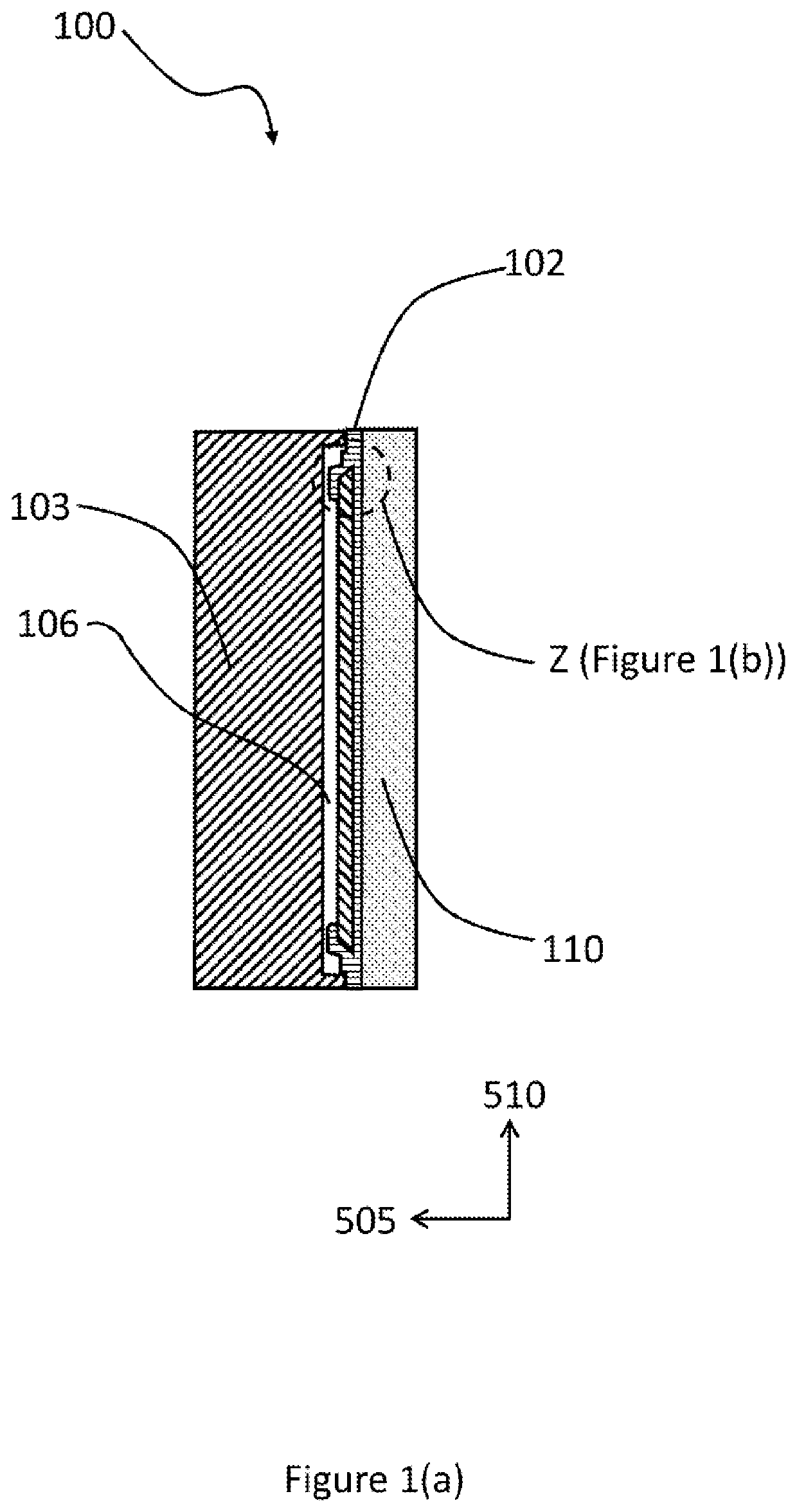
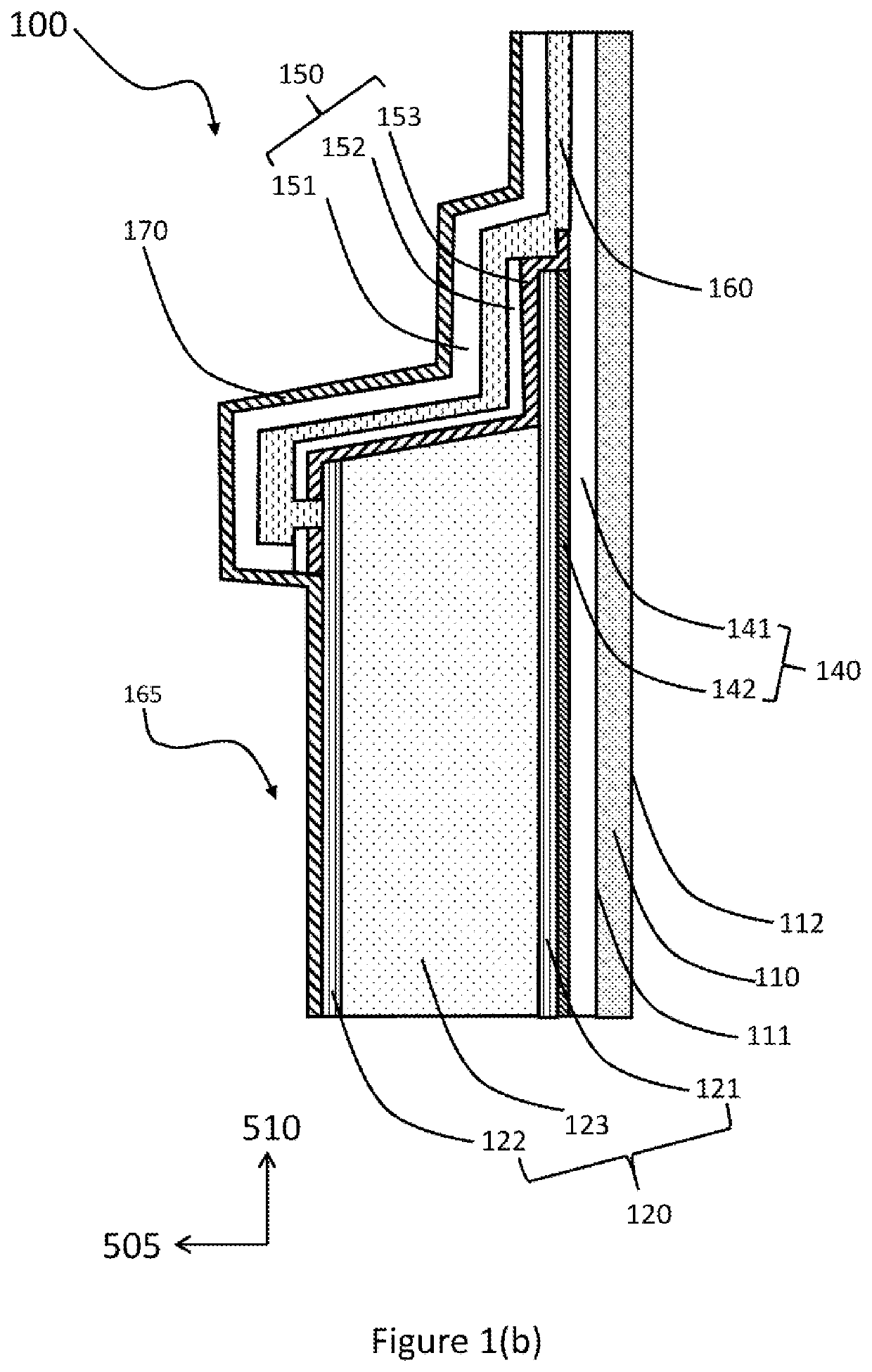
[0044]The insulated electrical component for a MEMS device of the first aspect comprises a substrate layer comprising first and second sides spaced apart in a thickness direction, wherein one or more electrical elements are arranged over the first side of the substrate layer.

[0045]The material of the substrate layer is not particularly limited. The substrate layer may be a silicon wafer or in other examples the substrate may be made of stainless steel, magnesium oxide (MgO), glass, nickel or the like. The substrate layer may be a laminate of two or more layers, where different layers may have the same or different composition. In some embodiments, the substrate comprises an uppermost layer which is in contact with the electrical element and which comprises silicon oxide, silicon nitride or the like. One or more lower layers of the laminate may be different from the uppermost layer and, for example, may comprise silicon wafer, MgO, stainless steel, glass or the like.

[0046]One or more...


PUM


Abstract

The present invention relates to an electrical component for a microelectromechanical systems (MEMS) device, in particular, but not limited to, an electromechanical actuator. In one aspect, the present invention provides an insulated electrical component for a microelectromechanical systems device comprising: i) a substrate layer comprising first and second sides spaced apart in a thickness direction; ii) one or more electrical elements arranged over the first side of the substrate layer, wherein each of the one or more electrical elements comprises: a) a ceramic member; and b) first and second electrodes disposed adjacent the ceramic member such that a potential difference may be established between the first and second electrodes and through the ceramic member during operation; iii) a continuous insulating layer, or laminate of insulating layers, arranged to overlie each of the one or more electrical elements arranged on the first side of the substrate layer; and iv) a passivation layer, or laminate of multiple passivation layers, disposed adjacent to, and at least partially overlying, each of the one or more electrical elements so as to provide electrical passivation between the first and second electrodes of each of the one or more electrical elements; wherein: a) the passivation layer, or at least an innermost layer of the laminate of multiple passivation layers which is disposed adjacent each of the one or more underlying electrical elements, is discontinuous; and / or b) the laminate of multiple passivation layers is recessed at a side which faces away from each of the underlying electrical elements, wherein a recess is provided in a region overlying each of the one or more electrical elements, such that the laminate of passivation layers is thinner in a thickness direction across the recess compared to other non-recessed regions of the laminate of passivation layers.

Description

[0001]The present invention relates to an electrical component for a microelectromechanical systems (MEMS) device, in particular, but not limited to, an electromechanical actuator. It may find particularly beneficial application as an actuator element for a droplet deposition head.[0002]Droplet ejection heads are now in widespread usage, whether in more traditional applications, such as inkjet printing, or in 3D printing, or other materials deposition or rapid prototyping techniques. Accordingly, the fluids may have novel chemical properties to adhere to new substrates and increase the functionality of the deposited material.[0003]Recently, inkjet printheads have been developed that are capable of depositing ink directly onto ceramic tiles, with high reliability and throughput. This allows the patterns on the tiles to be customized to a customer's exact specifications, as well as reducing the need for a full range of tiles to be kept in stock.[0004]In other applications, inkjet prin...

Claims


Application Information

Patent Timeline
IPC IPC(8): H01L41/053B41J2/14B41J2/16H01L41/047H01L41/08H01L41/09H01L41/187B81B3/00
CPCH01L41/0533B41J2/14201B41J2/1623B41J2/1628H01L41/0471B81B2203/04H01L41/0973H01L41/1876H01L41/1878B81B3/0021B81B2201/057H01L41/0815B41J2/1646B41J2/1642B41J2/1607B41J2202/03B41J2/1629B41J2/1643B41J2/1631H10N30/883H10N30/2047H10N30/8561H10N30/8554H10N30/078H10N30/708H10N30/871
Inventor VELLA, ANDREWMARDILOVICH, PETER
Owner XAAR TECH LTD
Learn More