MONOLAYER GRAPHENE ON NON-POLAR FACE SiC SUBSTRATE AND CONTROL METHOD THEREOF

a monolayer graphene and substrate technology, applied in the field of monolayer graphene on non-polar face sic substrate and control method thereof, can solve the problems of increasing the difficulty of subsequent manufacturing of semiconductor devices, not fully suitable for and difficult to fit with modern planarized electronic processing technology

Pending Publication Date: 2022-04-21
TIANJIN UNIV
View PDF1 Cites 0 Cited by
  • Summary
  • Abstract
  • Description
  • Claims
  • Application Information

AI Technical Summary

Problems solved by technology

However, this method is difficult to fit with modern planarized electronic processing technology, mainly because the graphene structure must growth on the side wall, which means SiC substrate must be subjected to longitudinal nano-scale micro-nano processing and subsequent heat treatment to obtain the sidewall graphene growth.
But modern semiconductor processing is not fully suitable for the mature process of SiC three-dimensional nano-mechanical processing, and at the same time, since all the sidewall graphene is grown on the three-dimensional sidewall, the subsequent manufacturing of semiconductor devices increases a lot of difficulty.

Method used


Image

  • MONOLAYER GRAPHENE ON NON-POLAR FACE SiC SUBSTRATE AND CONTROL METHOD THEREOF
  • MONOLAYER GRAPHENE ON NON-POLAR FACE SiC SUBSTRATE AND CONTROL METHOD THEREOF
  • MONOLAYER GRAPHENE ON NON-POLAR FACE SiC SUBSTRATE AND CONTROL METHOD THEREOF

Examples


embodiment 1

on-Polar Face SiC Substrate Cutting

[0068]A method for accurately cutting arbitrary angle non-polar crystal face SiC, including the following steps.

[0069](1) It is necessary to determine the included angle between the required non-polar crystal face and the (0001) plane. In this embodiment, the non-polar crystal face is (1105) plane, which forms an included angle of 37.1° with the (0001) plane; and different non-polar crystal faces correspond to different angles in other embodiments.

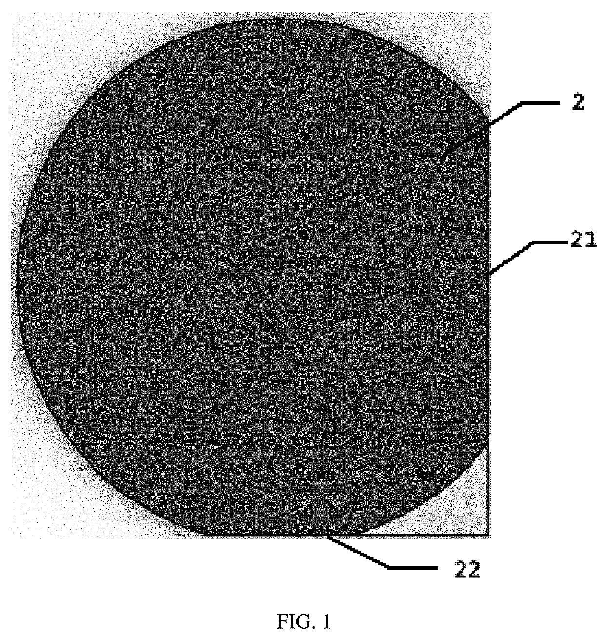
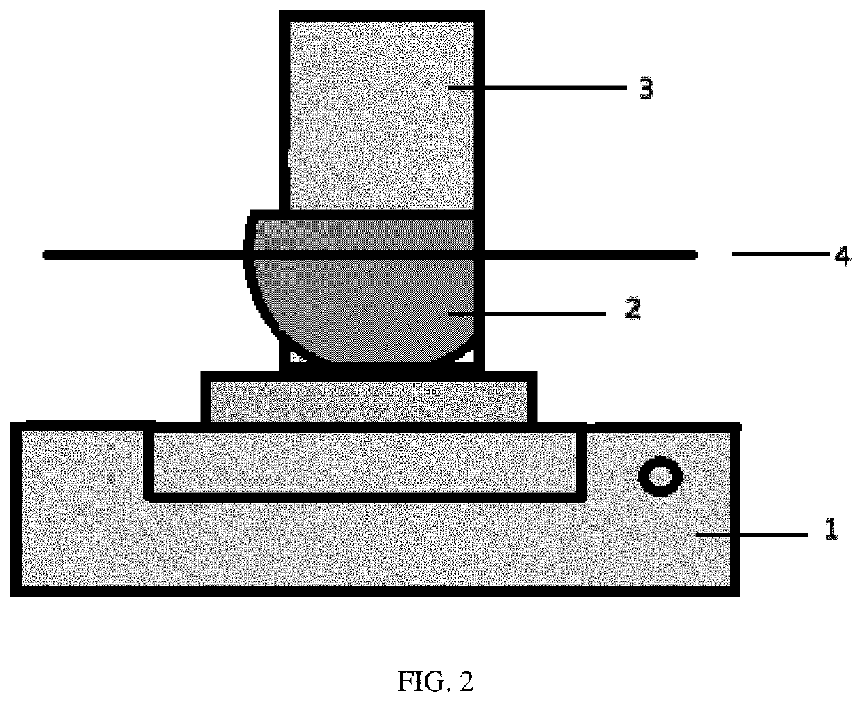
[0070](2) A fixture 1 is adopted to fix a SiC crystal column 2, as shown in FIG. 1, the SiC crystal column 2 has two mutually perpendicular reference planes 21 and 22. As shown in FIG. 2, a steel plate 3 is vertically arranged on the fixture 1 which can rotate 360° in the horizontal plane. The fixture 1 is required to maintain horizontal state before fixing the SiC crystal column 2, and the steel plate is in a vertical state.

[0071]When fixing the SiC crystal column 2, it is necessary to align the two mutu...

embodiment 2

on-Polar Face SiC Substrate Grinding and Polishing

[0074]A grinding and polishing method that can obtain non-polar crystal faces at arbitrary angle of SiC substrate with atomic flatness, the specific steps are as follows:

[0075](1) Pasting the SiC wafer (cut in the Embodiment 1) with paraffin wax on the power head disk, and then grinding it on the polishing machine; wherein the grinding disk is diamond grinding plate, adopting the grinding plates with diamond particle sizes of 60 μm and 30 μm for polishing the SIC wafer, respectively; where the polishing pressures was gradually increased from 100 to 200N during the grinding process, and the speed of the power head and the rotating speed of the grinding disc are 60 r / min and 280 r / min, respectively. During grinding process, the water flow is kept flushing to reduce the heat which caused by friction during the grinding process.

[0076](2) In mechanical polishing, diamond suspensions with diamond particle sizes of 3 μm and 1 μm are adopted...

embodiment 3

rowth Large Scale Graphene on Monolayer Non-Polar Crystal Face

[0081]Based on the concept of natural periodic in-situ growth of the substrate to manipulate the properties of graphene, the present invention proposed the method for growing large-area monolayer graphene on SiC substrate with non-polar crystal faces at arbitrary angle. The specific steps are as follows:

[0082](1) Pasting the SiC wafer (grinded and polished in the Embodiment 2) with paraffin wax on the ceramic, and then cut into a 3.5×4.5 mm non-polar crystal face SiC substrate for pretreating so as to remove the paraffin wax and complete cleaning;

[0083](2) putting the pretreated 3.5×4.5 mm non-polar crystal face SiC substrate in a new prepared graphite crucible, and then putting the graphite crucible in the heating position of the copper ring of the induction heating furnace;

[0084](3) in the first stage, heating the non-polar crystal face SiC substrate in vacuum environment at the temperature of 500° C. for 60 minutes;

[00...


PUM

PropertyMeasurementUnit
speedaaaaaaaaaa
diameteraaaaaaaaaa
particle sizeaaaaaaaaaa

Abstract

The present invention provides a control method to epitaxial growth monolayer graphene, in which a monolayer graphene is epitaxially grown on a non-polar crystal face at arbitrary angle of a non-polar crystal face SiC substrate, thereby utilizing the non-polar crystal face to manipulate the electrical transport properties of graphene. A monolayer graphene having ballistic transport properties can be epitaxially grown at arbitrary angle of non-polar crystal face SiC substrate by the above-mentioned control method.

Description

CROSS-REFERENCE TO RELATED APPLICATION[0001]This application is a national stage application of PCT / CN2019 / 076541. This application claims priority from PCT Application No. PCT / CN2019 / 076541, filed Feb. 28, 2019, the content of which is incorporated herein in the entirety by reference.TECHNICAL FIELD[0002]The present invention belongs to the field of semiconductor material, and particularly relates to a monolayer graphene on non-polar face SiC substrate and control method thereof.BACKGROUND OF THE PRESENT INVENTION[0003]With the rapid development of modern microelectronics technology, traditional silicon-based semiconductor electronic devices have been unable to suit more requirement, it is urgent to find a new basic material for electronic devices. Graphene is two-dimensional material composed of carbon atoms which arranged by hexagonal honeycomb, and it is considered to be a promising nano-electronic device material because of excellent mechanical, electronics, optical properties....

Claims


Application Information

Patent Timeline
Patent Type & Authority Applications(United States)
IPC IPC(8): H01L21/02C30B1/02C30B29/02B28D5/04
CPCH01L21/02013H01L21/02378H01L21/02433B28D5/045H01L21/0262C30B1/026C30B29/02H01L21/02527C23C16/02C23C16/26C30B29/36C30B33/00C30B1/02H01L21/02612H01L21/02024
Inventor MA, LEIDE HEER, WALTER ALEXANDERJI, PEIXUANZHANG, KAIMINZHAO, JIANZHAO, MEI
Owner TIANJIN UNIV
Why Eureka
Try Eureka