
Quantum device with multiplexed electrometer output signals

a quantum device and electrometer technology, applied in quantum computers, computing, instruments, etc., can solve the problems of limiting the massive use of inductors inside the cryostat, limiting the use of magnetic cores to promote the integration of inductors, and inter-inductor coupling can raise new problems, etc., to achieve the effect of introducing little quantization noise, low power consumption, and complex building

Pending Publication Date: 2022-06-16
COMMISSARIAT A LENERGIE ATOMIQUE ET AUX ENERGIES ALTERNATIVES +1
View PDF0 Cites 0 Cited by
  • Summary
  • Abstract
  • Description
  • Claims
  • Application Information

AI Technical Summary

Benefits of technology

The patent is about a way to mix and separate signals from electrometers. This is done by using excitation signals that are applied to each electrometer, which allows for the identification of a certain feature or characteristic with each electrometer and, ultimately, each quantum read. This is done by analyzing the output signals of the electrometers and finding the origin of these signals using the identifying characteristics. The patent also notes that it is advantageous to have the circuits for applying the excitation signals at the same temperature level as the demultiplexing circuit, as this simplifies the demultiplexing process. Additionally, the patent describes a technique called digital demultiplexing, which can be implemented with fewer demultiplexers and requires higher-frequency analog-to-digital converters and more complex digital demodulators. However, this method offers the advantage of providing more flexibility and is generally more efficient in practical implementations.

Problems solved by technology

Additionally, with this first read-out method, the use of magnetic cores to promote integration of the inductors is limited by the strong static magnetic field required to make the spin of the quasi-particles appear and which saturates magnetic permeabilities of the cores.
Air-core inductors do not face this problem, but they occupy a much larger surface area, limiting their massive use inside the cryostat.
Inter-inductor coupling can also raise new problems, when measuring qubits simultaneously using several of these inductors excited by reflectometry signals.
It is therefore not possible to use this solution to address a large number of qubits, for example a whole matrix of qubits, because it would be necessary either to output a number of wires at least equal to the number of qubits addressed, which requires a much too large space, or to arrange all the TIAs in the cryostat, which is not possible given the cooling capacities of the current cryostats (1 W maximum for operation at 4K, or 1 mW for operation at 100 mK).
Furthermore, the read-out speed of such a solution is limited by the capacitance of the wires (between 100 and 300 pF) to be charged upstream of the TIAs placed at room temperature.

Method used


Image

  • Quantum device with multiplexed electrometer output signals
  • Quantum device with multiplexed electrometer output signals
  • Quantum device with multiplexed electrometer output signals

Examples


first embodiment

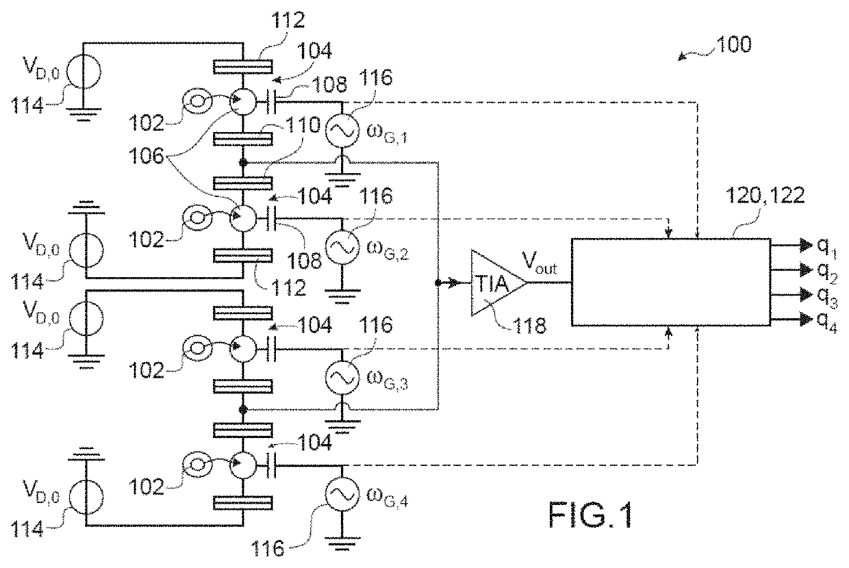
[0084]One exemplary embodiment of a quantum device 100 is described below in connection with FIG. 1.

[0085]The device 100 includes several spin qubits each comprising at least one quantum dot 102. In the exemplary embodiment shown in FIG. 1, four spin qubits are shown. However, the device 100 may include a different number of qubits, for example between 2 and 10,000 qubits.

[0086]The qubits in device 100 correspond to spin qubits made in a semiconductor layer, for example silicon or germanium. The charges whose spin is to be read out may correspond to electrons or holes.

[0087]The device 100 includes several electrometers 104 each electrostatically coupled to a potential well of the quantum dot 102 of one of the spin qubits. In the exemplary embodiment shown in FIG. 1, four electrometers 104 are shown.

[0088]Further, in the exemplary embodiment of FIG. 1, the electrometers 104 correspond to single electron transistors, or SETs. Each of the electrometers 104 includes a quantum dot 106 e...

second embodiment

[0134]One exemplary embodiment of a quantum device 100 is described below in connection with FIG. 12.

[0135]In this second embodiment, the qubits of the quantum device 100 are arranged as a matrix of M rows and N columns, with M and N being integers greater than or equal to 1 and at least one of the numbers M and N is strictly greater than 1. The electrometers 104 are also arranged by forming a matrix of M rows and N columns. This matrix of electrometers 104 is arranged above or below the matrix of qubits such that the quantum dot 102 of each of the qubits is electrostatically coupled to a quantum dot 106 of one of the electrometers 104 lying in proximity to, above or below, the quantum dot 102 of each of the qubits.

[0136]The matrix of qubits and the matrix of electrometers 104 can be made in a superimposed manner by implementing a 3D integration method.

[0137]The device 100 includes here M circuits 116 for applying at least one excitation signal to at least one input electrode of ea...


PUM


Abstract

A quantum device including:several spin qubits arranged as a matrix and each comprising a quantum dot;several electrometers each electrostatically coupled to a potential well of one of the quantum dots;circuits for applying an excitation signal to an input electrode of each electrometer, configured such that a value of the frequency, phase or maximum amplitude of each excitation signal is different from that of the other excitation signals, and applying a same excitation signal on electrometers coupled to a same row od qubits;a transimpedance amplifier having an input coupled to output electrodes of the electrometers;a demultiplexing circuit including an input electrically coupled to an output of the transimpedance amplifier, and configured to demultiplex the output signals to be delivered by the electrometers.

Description

TECHNICAL FIELD AND PRIOR ART[0001]The invention relates to the field of quantum devices, quantum information processing and quantum computing.[0002]Quantum computing is based on the use of a quantum state with two measurable levels as an information vector, called a qubit or quantum bit, and laws of quantum mechanics (superposition, entanglement, measurement) to execute algorithms. A quantum device, or calculator, with spin qubits makes it possible to manipulate quantum state of these qubits, especially in order to carry out operations.[0003]Unlike a so-called conventional electronic or computing machine (operating with two voltage levels defined as corresponding to binary states 0 and 1), a quantum device is similar to an analogue machine, in that the quantum state of qubits can take on an infinite number of values.[0004]Contemplated applications for quantum devices are numerous, from molecule simulation for medicine and the design of new vaccines and drugs to cryptography (implem...

Claims


Application Information

Patent Timeline
Patent Type & Authority Applications(United States)
IPC IPC(8): G06N10/40G06N10/20
CPCG06N10/40G06N10/20
Inventor MOREL, ADRIENBILLIOT, GÉRARDPILLONNET, GAËLMEUNIER, TRISTAN
Owner COMMISSARIAT A LENERGIE ATOMIQUE ET AUX ENERGIES ALTERNATIVES
Learn More