Plasma-enhanced chemical vapor deposited SIO2/SI3N4 multilayer passivation layer for semiconductor applications

a technology of chemical vapor deposited sio2/si3n4 and semiconductor integrated circuits, which is applied in the direction of natural mineral layered products, water-setting substance layered products, transportation and packaging, etc., can solve the problem of increasing the width of the spacing between metal lines and metal thickness, forming voids (keyholes), and affecting the performance of the produ

Inactive Publication Date: 2000-01-25
VANGUARD INTERNATIONAL SEMICONDUCTOR CORPORATION
View PDF5 Cites 70 Cited by
  • Summary
  • Abstract
  • Description
  • Claims
  • Application Information

AI Technical Summary

Problems solved by technology

Unfortunately, as the metal lines that form the interconnections are made closer together to satisfy the higher packing density for ULSI integrated circuits, the aspect ratio (the width of the spacings between metal lines to the metal thickness) increases.
This can result in the formation of voids (keyholes) in the nonconformal insulating or passivation layer between the metal lines when the passivation is deposited next.
Also because the silicon nitride has a higher stress than the silicon oxide, cracking of the silicon nitride layer is prevalent at the bottom corners in the recesses between the metal lines.
This results in the formation of voids 30 having a keyhole shape.
The incomplete removal of the residual photoresist then results in contamination and corrosion of the subsequent metal layer when the trapped photoresist outgases during the subsequent metal or alloy deposition step.
This is a particularly serious problem for 0.38 micrometer DRAM devices (0.38 um FET channel lengths) when the minimum spacings between the metal lines at the second metal level (M2) of interconnections are less than 0.575 um.
The passivation layer typically fails the pinhole test when the total thickness of the silicon oxide layer 22 and the silicon nitride layer 24 is less than 8000 Angstroms, but thicker passivation layers can present a keyhole problem.
One method for depositing a passivation layer is described by Lindenfelser in U.S. Pat. No. 4,692,786, in which a three-layer sandwich passivation coating is deposited directly on the silicon substrate to prevent ion contamination during the fabrication of bipolar transistors, but he does not address the above keyhole or Si.sub.3 N.sub.4 cracking problems.
Ang et al., U.S. Pat. No. 4,707,721, describe a method for making a passivated dual-gate system using a titanium nitride which is a good electrical conductor, but do not address the keyhole or cracking problem in a silicon nitride passivation layer.

Method used


Image

  • Plasma-enhanced chemical vapor deposited SIO2/SI3N4 multilayer passivation layer for semiconductor applications
  • Plasma-enhanced chemical vapor deposited SIO2/SI3N4 multilayer passivation layer for semiconductor applications
  • Plasma-enhanced chemical vapor deposited SIO2/SI3N4 multilayer passivation layer for semiconductor applications

Examples


Embodiment Construction

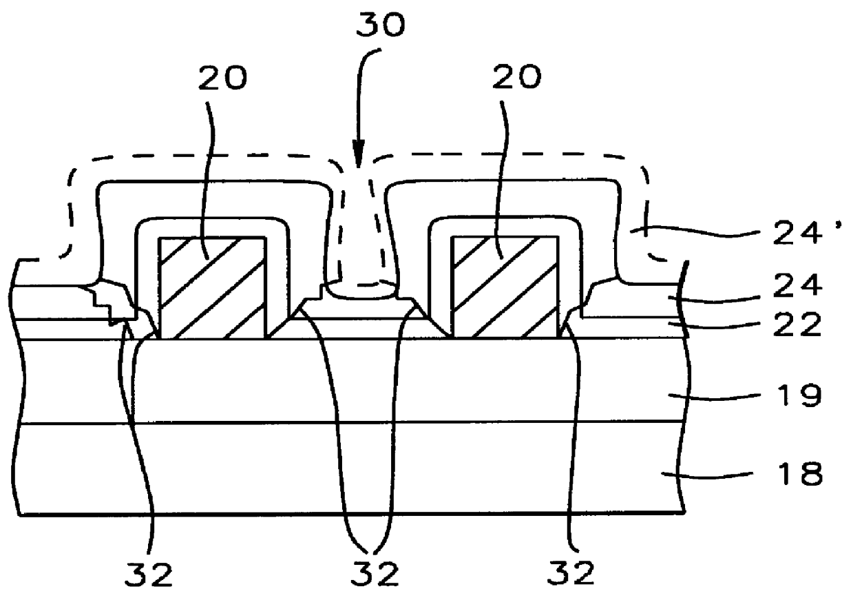
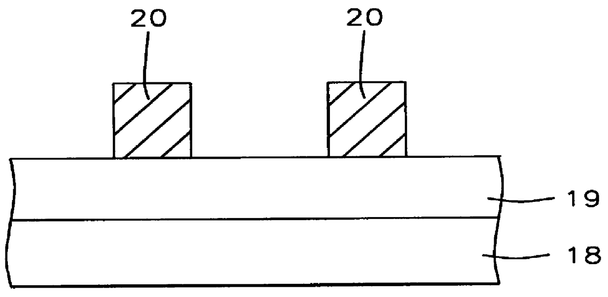
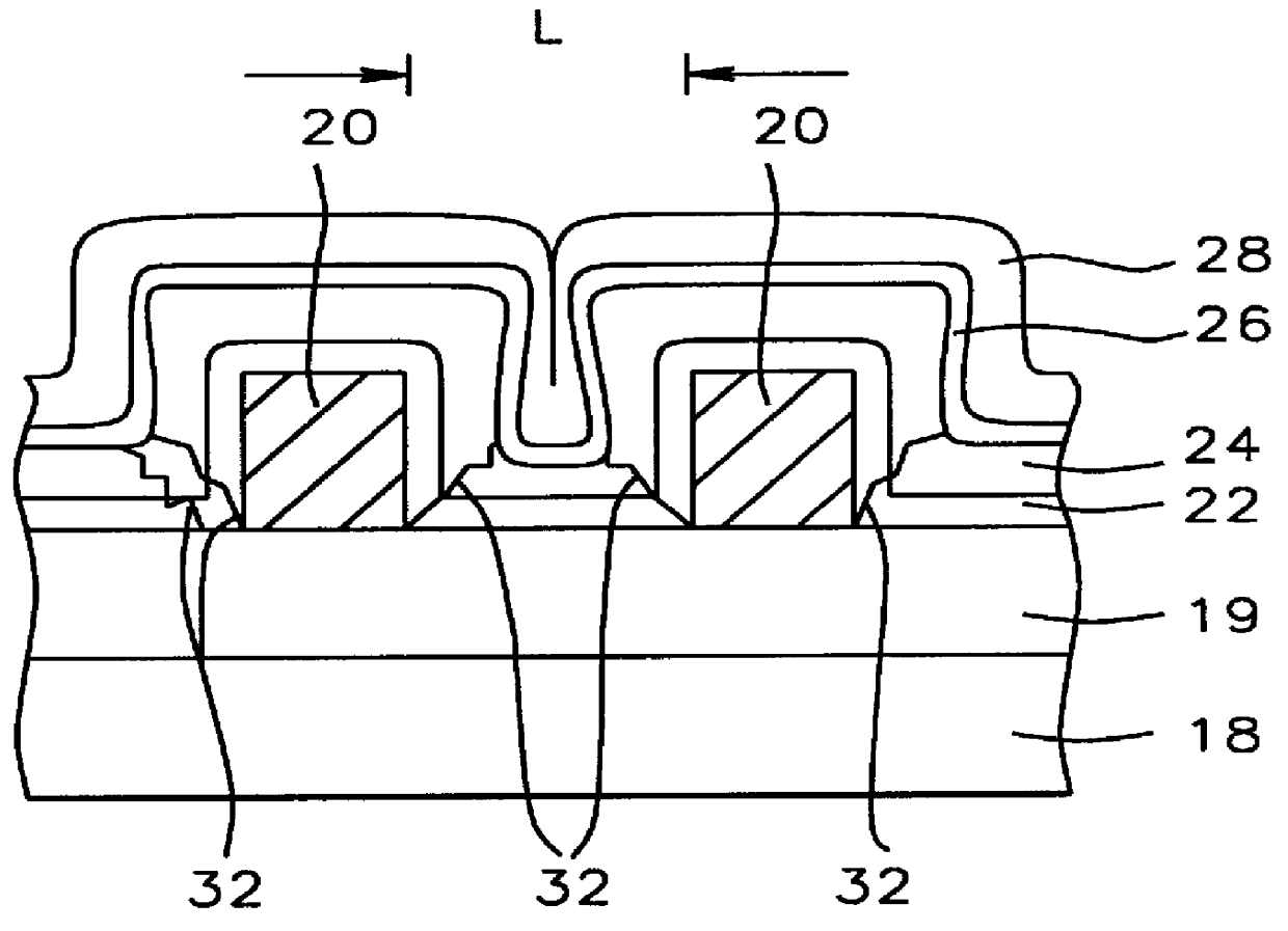
To verify the improvement in the number of pinholes, sample chips having the second metal pattern for a 16 megabit DRAM chip and the passivation multilayer as described above in the specification were tested. The passivation multilayer consisted of a first and a second SiO.sub.2 layer of 300 Angstroms each, a first Si.sub.3 N.sub.4 layer of 800 Angstroms, and a second Si.sub.3 N.sub.4 layer of 3800 Angstroms. The sample chips were subjected to a pressure-cooker test and a temperature-cycling test, and then a pinhole test was performed using 10% by weight of potassium hydroxide (KOH) in water at 45.degree. C. for 30 minutes, and were then visually inspected by noting the color change of the metal lines where pinholes occur. For the pressure-cooker test (PCT), the sample chips were subjected to an ambient having a pressure of 15 pounds per square inch (psi), at a temperature of 121.degree. C., and at a relative humidity of 100% for 96 hours and for 168 hours. 100% of the sample chips ...


PUM

PropertyMeasurementUnit
thicknessaaaaaaaaaa
thicknessaaaaaaaaaa
thicknessaaaaaaaaaa

Abstract

A method was achieved for forming a multilayer passivation layer comprised of a silicon oxide / silicon nitride / silicon oxide / silicon nitride by depositing the layers consecutively in a single PECVD system. The method consists of depositing a first SiO2 layer that serves as a stress-release layer, a thin Si3N4 layer that serves as a buffer layer that minimizes cracking and as a passivation layer that prevents mobile alkaline ion penetration, a thin second SiO2 layer to fill and seal any remaining cracks and pinholes in the first Si3N4 layer, and a main Si3N4 passivation layer that prevents water and / or other corrosive chemicals from attacking the metal. Since this multilayer passivation layer can be deposited essentially pinhole-free to a thickness that is less than the prior art's passivation layer of 8000 Angstroms needed to prevent pinholes, it can be used on 0.38 to 0.25 um DRAM technology, which eliminates voids that could otherwise trap photoresist which can later cause corrosion of the metal lines.

Description

(1) Field of the InventionThe present invention relates to a method for making a plasma-enhanced chemical vapor deposited (PECVD) silicon oxide / silicon nitride multilayer (stacked layer) as a passivation layer on semiconductor integrated circuits, and more particularly relates to a method for making an insulating / passivating layer over interconnecting metal lines on multilevel interconnections for integrated circuits.(2) Description of the Prior ArtMultilevels of metal interconnections are used on Ultra Large Scale Integration (ULSI) integrated circuits to wire-up the discrete semiconductor devices on the semi-conductor chips. The different levels of interconnections are separated by layers of insulating material, such as PECVD silicon oxide (SiO.sub.2) and silicon nitride (Si.sub.3 N.sub.4) layers. The silicon nitride also serves as a barrier layer or passivation layer to prevent contamination from moisture and other corrosive chemicals, and to prevent ionic contamination from ligh...

Claims


Application Information

Patent Timeline
Patent Type & Authority Patents(United States)
IPC IPC(8): H01L21/70H01L21/768H01L23/52H01L21/02H01L21/316H01L23/532H01L21/314H01L21/318
CPCH01L21/02164H01L21/022H01L21/02211H01L21/02274H01L21/3145H01L21/31612H01L21/3185H01L21/76832H01L21/76834H01L23/5329H01L21/0217Y10T428/24917H01L21/76837Y10S438/938H01L2924/0002H01L2924/00
Inventor TSAI, KWONG-JRCHENG, SHIANG-PENGTU, YEUR-LUENLIAW, ING-RUEY
Owner VANGUARD INTERNATIONAL SEMICONDUCTOR CORPORATION
Why Eureka
Try Eureka