Dual work function CMOS device

Inactive Publication Date: 2000-02-22
IBM CORP
View PDF19 Cites 44 Cited by
  • Summary
  • Abstract
  • Description
  • Claims
  • Application Information

AI Technical Summary

Problems solved by technology

This leads to a multiplication of the alignment problems involved with each resist patterning step and increased throughput time because of the additional definition steps and two separate implantation st

Method used


Image

  • Dual work function CMOS device
  • Dual work function CMOS device
  • Dual work function CMOS device

Examples


Embodiment Construction

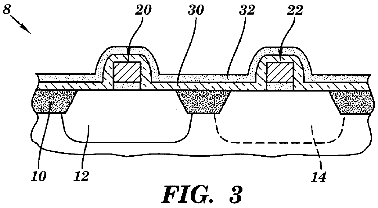
Referring to the FIGS. 1-6, there is shown a stepwise series of schematic views of the process and integrated circuit (IC) chip 8 of preferred embodiments of the present invention. A cross section of the IC chip 8 is shown in FIG. 1. The chip 8 itself is typically a P+ substrate, in which isolation areas may have been formed, either shallow trench isolation areas 10 or semi-recessed oxide isolation (S-ROX) structures. Between these areas, active areas are formed. The active areas commonly include n-wells 12, p-wells 14, or the doped substrate itself. The well structures 12,14 are implanted in the usual fashion and then a gate oxide 16 is grown on the surface. On top of gate oxide layer 16, an undoped polysilicon 18 layer is deposited to form the structure shown in FIG. 1.

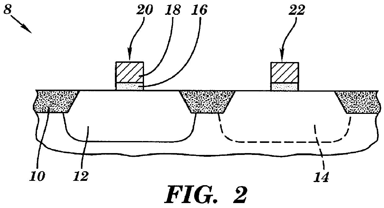
As shown in FIG. 2, gates 20, 22 are defined using the conventional method, which comprises depositing a layer of a photosensitive material, known as a resist, exposing the photosensitive material to an energy sourc...


PUM


Abstract

A dual work function CMOS device and method for producing the same is disclosed. The method includes: depositing a first layer of a doped material, either n-type or p-type, over a substrate to be doped; defining the areas that are to be oppositely doped; depositing a second layer of an oppositely doped material over the entire surface; and subjecting the entire CMOS device to a high temperature, drive-in anneal. The drive-in anneal accelerates the diffusion of the dopants into the adjacent areas, thereby doping the gate polysilicon and channels with the desired dopants. A nitride barrier layer may be utilized to prevent the second dopant from diffusing through the first layer and into the substrate beneath.

Description

1. Technical FieldThis invention relates generally to a method of manufacturing integrated circuit (IC) chips and the IC chips produced thereby. More specifically, the present invention relates to a dual work function complementary metal oxide semiconductor (CMOS) device and a method for producing these devices.2. Background ArtPresently, integrated circuit chips are manufactured by beginning with a wafer. If desired, these wafers may be grown with a given type of impurity, depending upon whether one desires electron acceptors (p-type impurities) or electron donors (n-type impurities) in the wafer.One of the first processing steps of the wafer in forming an integrated circuit (IC) chip is the creation of device isolation. Shallow trench isolation areas may be formed by defining areas with a photoresist and reactive ion etching to form the shallow trenches. The shallow trenches are then filled with a nonreactive silicon oxide and planarized by a chemical mechanical polish. In some ca...

Claims


Application Information

Patent Timeline
IPC IPC(8): H01L21/70H01L21/8238
CPCH01L21/823842Y10S257/90
Inventor FRENETTE, ROBERT O.HALLOCK, DALE P.MONGEON, STEPHEN A.SPERANZA, ANTHONY C.TONTI, WILLIAM R. P.
Owner IBM CORP
Why Eureka
Try Eureka