Optical plasmon-wave structures

a technology of optical plasmon wave and structure, applied in non-linear optics, instruments, optics, etc., can solve the problems of power coupling variation between the spw and the optical wave, modulation of the optical wave, and inability to develop a practical optical spw modulator which could be commercialized,

Inactive Publication Date: 2000-03-07
VERIFIBER TECH
View PDF8 Cites 96 Cited by
  • Summary
  • Abstract
  • Description
  • Claims
  • Application Information

AI Technical Summary

Problems solved by technology

These propagation constant variations result in power coupling variation between the SPW and the optical wave and consequently modulation of the optical wave.
However, attempts to develop a practical optical SPW modulator which could be commercialized have not been successful.
All of foregoing presently exhibit inferior performance, manufacturability and design flexibility to the alternative technologies.
The deficiencies of this sandwich design are caused primarily by an attempt to combine the modulator control structure with the surface plasmon wave generation and support structure.
The combination of these two functions puts severe design constraints on the thickness of the metal layer in which the SPW must be generated.
High resistance increases the input voltage for a desired modulation depth and generates heat which is highly undesirable.
If intense enough, such heating may damage the metal layer or the EO layer with which the metal layer may be in contact.
Particularly vulnerable to heat damage are thin polymer EO layers.
These two design constraints are often in conflict and may prevent a pragmatic solution at the modulation bandwidth desired and at the wavelength desired for the guided wavevector.
Still further, the use of this structure as a modulator is limited because the modulation electrodes act as a parallel plate capacitor.
This electrode configuration has high capacitance which greatly limits the overall bandwidth.
These constraints make it even more difficult to design efficient SPW generation and support structures, particularly if modulation electrode constraints must be simultaneously satisfied.
These coupling techniques have limited effects since the range of design parameters is narrow.

Method used


Image

  • Optical plasmon-wave structures
  • Optical plasmon-wave structures
  • Optical plasmon-wave structures

Examples


Embodiment Construction

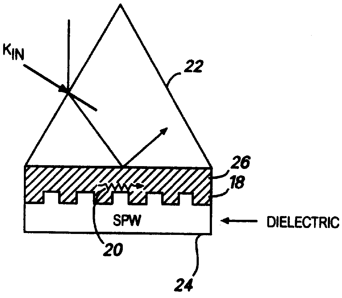
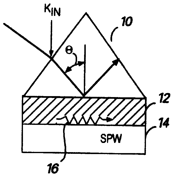
FIG. 1 illustrates a prior art method of generating a surface plasmon wave. A high index optical prism 10 is used with a thin metal layer 12 evaporated on its base and mounted on a dielectric base 14.

The incident light wavevector, at wavelength .lambda., inside the prism 10 is:

K.sub.IN =n.sub.P sin.theta.2.pi. / .lambda.

where n.sub.p is the prism refractive index and .theta. is the angle of incidence. The evanescent electromagnetic field from the incident TM polarized light penetrates the metal layer 12 and when an angle .theta..sub.SPW satisfies the matching condition:

n.sub.p sin .theta..sub.SPW 2.pi. / .lambda.=K.sub.SPW =.theta..sub.SPW 2.pi. / .lambda.

then a SPW 16 is generated in the metal layer 12. As previously described .beta..sub.SPW is the propagation constant of the SPW and depends on the refractive index and thickness of the metal layer 12. Since the SPW is excited via the evanescent fields of the lightwave, this method will be termed evanescent coupling.

According to one prefe...


PUM

PropertyMeasurementUnit
refractive indexaaaaaaaaaa
frequenciesaaaaaaaaaa
refractive indexaaaaaaaaaa

Abstract

Optical plasmon-wave attenuator and modulator structures for controlling the amount of coupling between an guided optical signal and a surface plasmon wave. Optical power coupled to the plasmon wave mode is dissipated in varying amounts producing an intensity modulation effect on the optical signal. For electrical modulation, an additional dielectric (or polymer) layer with variable refractive index in optical contact with a metal layer supporting at least one plasmon wave mode is used to perturb or vary the propagation constant of plasmon wave. Propagation constant variation results in the power coupling variation between the surface plasmon wave and the optical wave. The refractive index variation of the dielectric (or polymer) layer can be accomplished via an electro-optic traveling-wave, a lump-element, or any other integrated optics modulator configuration situated to affect the layer, thereby permitting data rates into tens of GHz. Because of the extremely small interaction lengths needed, the optical plasmon-wave modulator is a very compact device which can be implemented on the top of a fiber or as an integrated optical planar structure.

Description

1. Field of the InventionThe present invention generally relates to an optical structures and methods of making such structures, and more particularly, to an optical structures including attenuators and modulators which vary the intensity of a guided lightwave by controlling the amount of power coupling between a guided light mode and a surface plasmon wave mode.2. Description of Background ArtA surface plasmon wave (SPW) is an electromagnetic wave which propagates along the interface between two materials having dielectric constants of opposite signs, e.g., a metal and a dielectric layer. The polarization of a SPW is transverse magnetic (TM) since its electric field is perpendicular to the propagation interface. SPWs can be analyzed by techniques used for TM optical modes since they obey identical field equations and satisfy the same boundary conditions. Unique features of SPWs are that almost all of their energy is concentrated at the dielectric / metal interface and their propagati...

Claims


Application Information

Patent Timeline
Patent Type & Authority Patents(United States)
IPC IPC(8): G02F1/01G02F1/19
CPCG02F1/011G02F1/195G02F2203/10
Inventor ANEMOGIANNIS, EMMANUEL
Owner VERIFIBER TECH
Why Eureka
Try Eureka