Pyroelectric infrared sensor device

a sensor device and infrared technology, applied in the field of solid-state microelectronics, can solve the problems of reducing the durability of thermal shocks, noise, and mechanical or physical strength, and achieve the effects of avoiding problems, improving sensitivity and relative detection rate, and low cos

Inactive Publication Date: 2000-04-11
MURATA MFG CO LTD
View PDF7 Cites 31 Cited by
  • Summary
  • Abstract
  • Description
  • Claims
  • Application Information

AI Technical Summary

Benefits of technology

Another advantage of the invention is that the pyroelectric infrared sensor device having comb-shaped electrodes is capable of avoiding the problems faced by the conventional techniques and also by sensor modules making use of the same.
is that the pyroelectric infrared sensor device having comb-shaped electrodes is capable of avoiding the problems faced by the conventional techniques and also by sensor modules making use of the same.
It is a further advantage that the improved pyroelectric infrared sensor device having comb-shaped electrodes is capable of further improving the sensitivity and relative detection rate while simultaneously enabling mass production at low cost.
To attain the foregoing advantages, the disclosed pyroelectric infrared sensor device includes a substrate made of a pyroelectric material, comb-shaped electrodes formed as a pair on one principal plane of the substrate serving as an infrared light sensitive surface, and an electrode formed on the opposite principal plane of the substrate and having a portion insulatively overlapping the comb-shaped electrodes. Each comb-shaped electrode may have three or more electrode-pairs, allowing the pyroelectric material to be polarized upon application of an appropriate voltage.
With the principles of the invention, since the substrate is polarized by the comb-shaped electrodes, thermal or heat energy of incoming infrared light is captured only at the one principal surface of the substrate serving as the infrared light receiving plane. Accordingly, an intended pyroelectric current may be obtainable due to heat exchange only at or near such one principal surface of the substrate.
In addition, since the opposite electrode disposed on the remaining principal plane of the substrate has a certain portion opposing or overlapping the comb-shaped electrodes, it becomes possible to improve dipole concentration between the comb-shaped electrodes, which may in turn increase the polarization rate of the substrate. This has been found out by simulation results using the finite element method. It is also possible by increasing the polarization rate of the substrate to increase the electrical capacitance (electrostatic capacitance) of the device structure of the pyroelectric infrared sensor.

Problems solved by technology

This would result in a decrease in mechanical or physical strength while simultaneously reducing durability against thermal shocks applied thereto.
As far as performance is concerned, the pyroelectric body can directly receive external vibrations, mechanical shocks, and thermal shocks due to strong infrared light illumination, causing the pyroelectric infrared sensor device per se to receive mechanical vibrations, which in turn results in occurrence of noise.
In short, since the thickness of pyroelectric infrared sensor device is reduced, rendering the resultant structure mechanically weakened, the mechanical and thermal reliability is undesirably degraded thus making the handling of pyroelectric infrared sensor devices very difficult.
In addition, the reduction in thickness of pyroelectric devices can increase the risk of occurrence of malfunctions due to the piezoelectric effect of the pyroelectric body per se.
This might lead to a reduction in reliability.
Therefore, it is difficult for the prior art pyroelectric infrared sensor modules 101, 201 to attain excellent performance with the S / N ratio enhanced.
With regard to fabrication, the mechanical or physical weakness of the pyroelectric body per se renders difficult both rigid support of the pyroelectric device and its retention in an accurate position during fabrication.
More practically, it becomes difficult to accurately mount and support the pyroelectric sensor device by adhesion on an associated substrate at an intended location.
This would also affect performance.
A further problem encountered with the conventional techniques is that specific thermal insulation (thermal resistivity) schemes are required for rendering the light-receiving section hollow in shape thus making it unable to easily form the pyroelectric light-receiving section.
Moreover, because in most cases the thickness of the pyroelectric body per se is designed to fall within the range of 70 to 100 micrometers, for example, the resulting yield of production is lowered rendering extremely difficult the manufacture of such pyroelectric infrared sensor device itself.
A still further problem faced with the conventional techniques is an increase in manufacturing cost due to an increase in the number of parts or components required.
Unfortunately, the above advantage of the conventional pyroelectric infrared sensor device 5 shown in FIG. 15 does not come without accompanying serious problems, which follow.
While it is no longer necessary to make thinner the pyroelectric substrate per se, the area of its light-receiving section as well as th e electric capacitance (electrostatic capacitance) thereof remain less, rendering it difficult to obtain a sufficient pyroelectric current while also placing certain limitations on the possible improvement in sensitivity and in relative detection rate.
Another problem in the conventional techniques is that the electric capacitance (electrostatic capacitance) remains smaller so that high-frequency noise components such as white noise are increased undesirably.
It has advantages, but is not able to avoid the foregoing disadvantages of conventional pyroelectric infrared sensor devices.

Method used


Image

  • Pyroelectric infrared sensor device
  • Pyroelectric infrared sensor device
  • Pyroelectric infrared sensor device

Examples


first embodiment

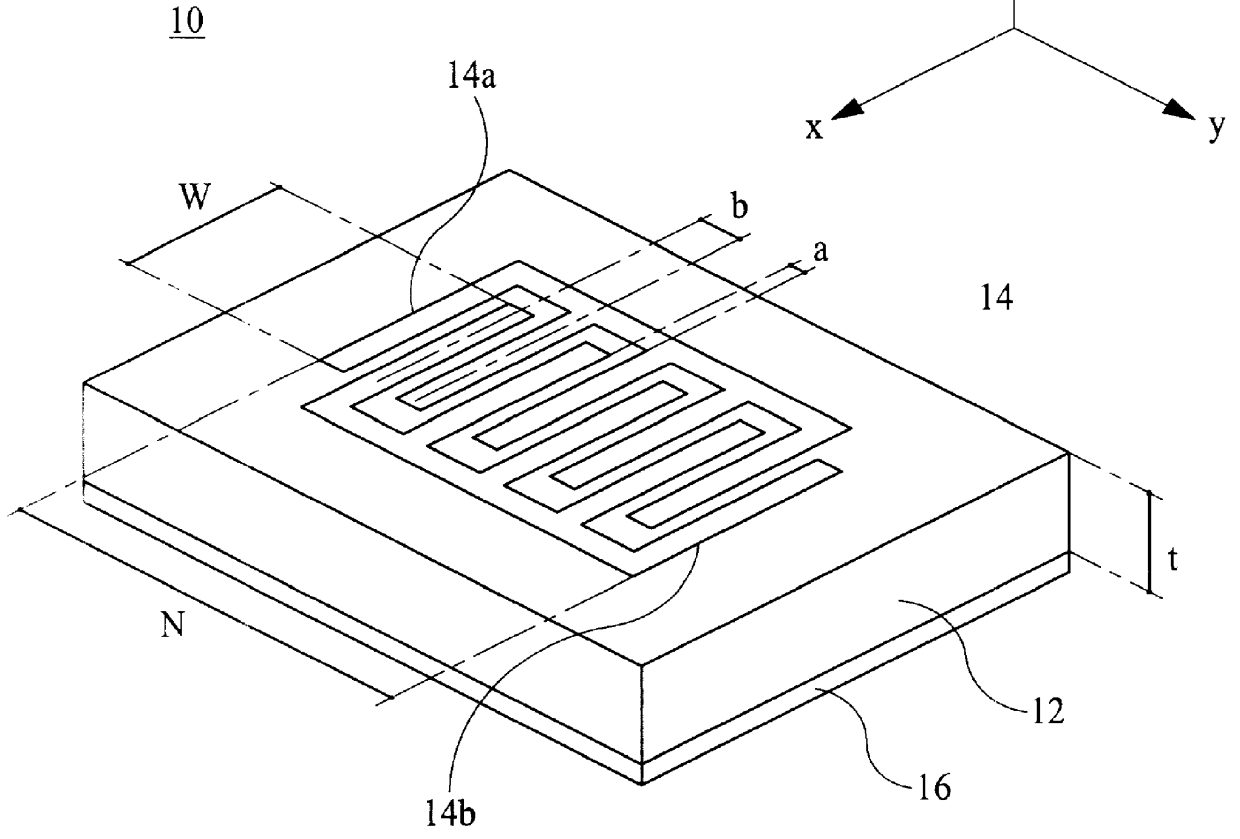
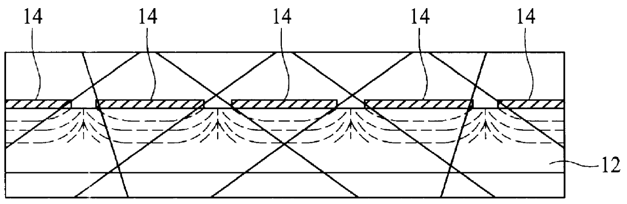
Referring to FIG. 1, a pyroelectric infrared sensor device in accordance with a first embodiment is generally designated by numeral 10. This sensor device 10 includes a substrate 12 of a rectangular shape with the thickness t. The substrate 12 may be made of a chosen pyroelectric material. Preferably, this material is lower in pyroelectricity along the thickness of substrate 12 than along its surface in order to provide a greater output voltage at the surface of substrate 12. This may be met by use of tetragonal-system lead titanate pyroelectric ceramics for substrate 12.

A pair of comb-shaped electrode patterns 14 are disposed on the top surface of the substrate 12 in such a manner that each has a specifically selected number of substantially equally spaced, parallel conductive open-ended "finger" portions. More specifically, one comb-shaped electrode 14 is patterned to have five equal-spaced, open-ended fingers 14a which are consecutively shorted to each other at one end and remain...

second embodiment

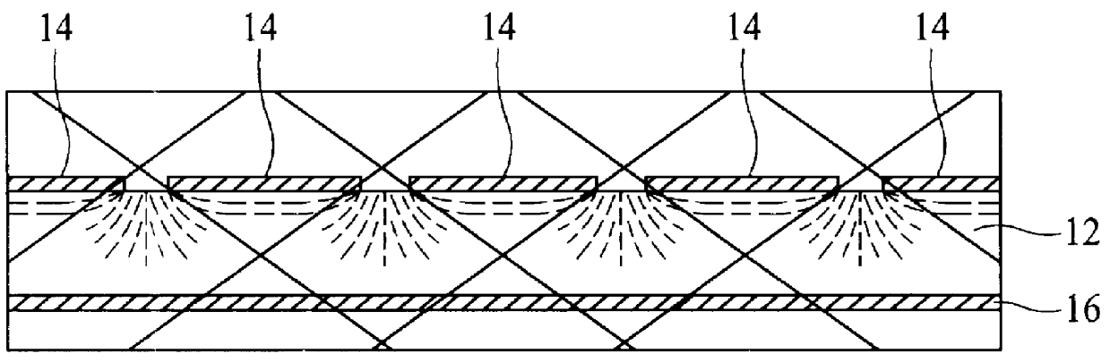
Turning now to FIG. 3, a pyroelectric infrared sensor module structure in accordance with the invention is generally designated by numeral 30. This sensor module 30 includes a pyroelectric infrared sensor device 20 mounted on a support base plate 32 called the stem. The sensor device 20 is similar to that shown in FIG. 1 with a series combination of two comb-shaped electrode pairs 24, 26 patterned on a pyroelectric substrate 22 of rectangular planar shape. The sensor device 20 with such serially coupled comb-shaped electrode pairs 24, 26 may be called the "dual comb-shaped electrode sensor" in some cases.

More specifically, as shown in FIG. 3, the pyroelectric infrared sensor device 20 includes on the top surface of the pyroelectric substrate 22 two pairs of comb-shaped electrodes 24, 26, each of which electrodes has five parallel open-ended fingers spatially mated or interdigitated in relation to those of its associated comb-shaped electrode on substrate 22. These comb-shaped electr...

embodiment 30

Still another advantage of the embodiment 30 is that since the opposite electrode 28 having portions insulatively overlapping the comb-shaped electrode pairs 24, 26 is on the bottom surface of the substrate 22, the electric resistance of the pyroelectric infrared sensor device 20 can be further decreased as a whole.

Therefore, it becomes possible to eliminate use of an external resistor to be provided between the gate (G) of FET 34 and the ground (GND). Note here that the resistor Rg in the electrical equivalent circuit diagram of FIG. 4 can be a mere symbolic representation of the inherent resistance of pyroelectric infrared sensor device 20, and not any discrete element to be separately coupled thereto.

Yet another advantage of module 30 is that the pyroelectric infrared sensor device 20 used therein does not operationally depend upon the thickness direction of the pyroelectric substrate 22; therefore, it is no longer necessary for substrate 22 to be much reduced in thickness. Accor...


PUM


Abstract

A pyroelectric infrared sensor device with improved sensitivity and relative detection rate and reduced manufacturing cost. The infrared sensor device includes a substrate of rectangular shape. The substrate is made of a pyroelectric material, such as tetragonal-system lead titanate pyroelectric ceramics. A pair of comb-shaped electrode patterns each having a set of parallel conductive open-ended fingers are disposed on the top surface of the substrate such that the open-ended fingers of one electrode pattern are spatially interdigitated in relation to those of the other. The paired comb-shaped electrodes have at least three finger pairs whereas the interelectrode distance corresponding to the gap between neighboring fingers is greater than 100 micrometers. These comb-shaped electrodes satisfying the criteria render the pyroelectric material, upon application of a DC voltage between them, substantially horizontally polarizable at or near the top substrate surface which acts as the infrared light receiving plane. An opposite electrode is on the entire bottom surface of the substrate. This electrode has portions insulatively overlapping the comb-shaped electrodes with the pyroelectric material being sandwiched therebetween.

Description

1. Field of the InventionThe present invention relates generally to solid-state microelectronics, and more particularly to pyroelectric radiation sensitive devices. The invention also relates to pyroelectric infrared light sensor structures adaptable for use with sensor packages or modules for detecting the presence of a human body in several applications including, but not limited to, alarm systems, intelligent air conditioners, autoadjustable illumination apparatus, and auto power-on audio systems.2. Description of the Related ArtOne conventionally known pyroelectric infrared sensor device is designated by the numeral 1 in FIG. 11. This infrared sensor device 1 includes electrodes 2a, 3a which are formed on the top and bottom surfaces of a rectangular-shaped pyroelectric body 1a with polarization being vertically effected between the electrodes 2a, 3a along the thickness as indicated by arrows shown. The electrodes 2a, 3a are disposed in the direction at right angles to the polari...

Claims


Application Information

Patent Timeline
Patent Type & Authority Patents(United States)
IPC IPC(8): G01J5/10G01J5/02G01J5/34G01J5/12H01L37/00H01L37/02G01J1/02H01L35/00
CPCG01J5/02G01J5/024G01J5/04G01J5/046G01J5/06G01J5/10G01J5/34H01L37/02H01L2224/48091H01L2924/00014H10N15/10
Inventor ITO, SATORU
Owner MURATA MFG CO LTD
Why Eureka
Try Eureka