Dynamic random access memory fabricated with SOI substrate

a random access memory and soi substrate technology, applied in the direction of capacitors, semiconductor devices, electrical devices, etc., can solve the problems of deteriorating step coverage in the contact hole or the like, difficult patterning process on the upper layer, and difficult patterning process such as the bit line 35 or the lik

Inactive Publication Date: 2000-06-06
SONY CORP
View PDF2 Cites 18 Cited by
  • Summary
  • Abstract
  • Description
  • Claims
  • Application Information

AI Technical Summary

Benefits of technology

Accordingly, it is an object of the present invention to provide an improved semiconductor memor

Problems solved by technology

However, since the conventional semiconductor memory device has the multilayer structure in which several polycrystalline silicon layer are stacked on the silicon substrate 32, a step at the contact portion in the memory cell portion is increased so that a step coverage in the contact hole or the like is deteriorated.
There is then the disadvantage that the patterning-process on the upper layer, e.g.,

Method used


Image

  • Dynamic random access memory fabricated with SOI substrate
  • Dynamic random access memory fabricated with SOI substrate
  • Dynamic random access memory fabricated with SOI substrate

Examples


Embodiment Construction

The present invention will now be described with reference to FIGS. 2 through 5.

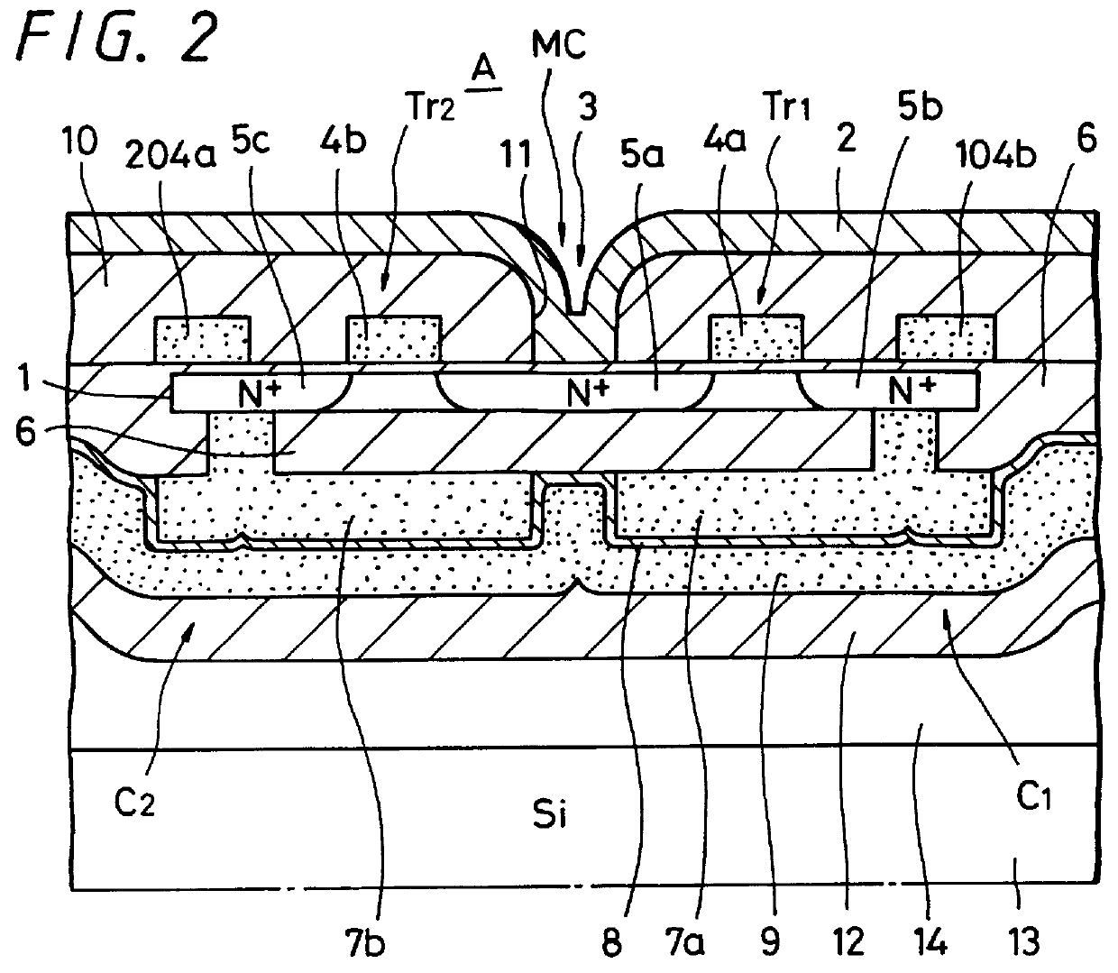
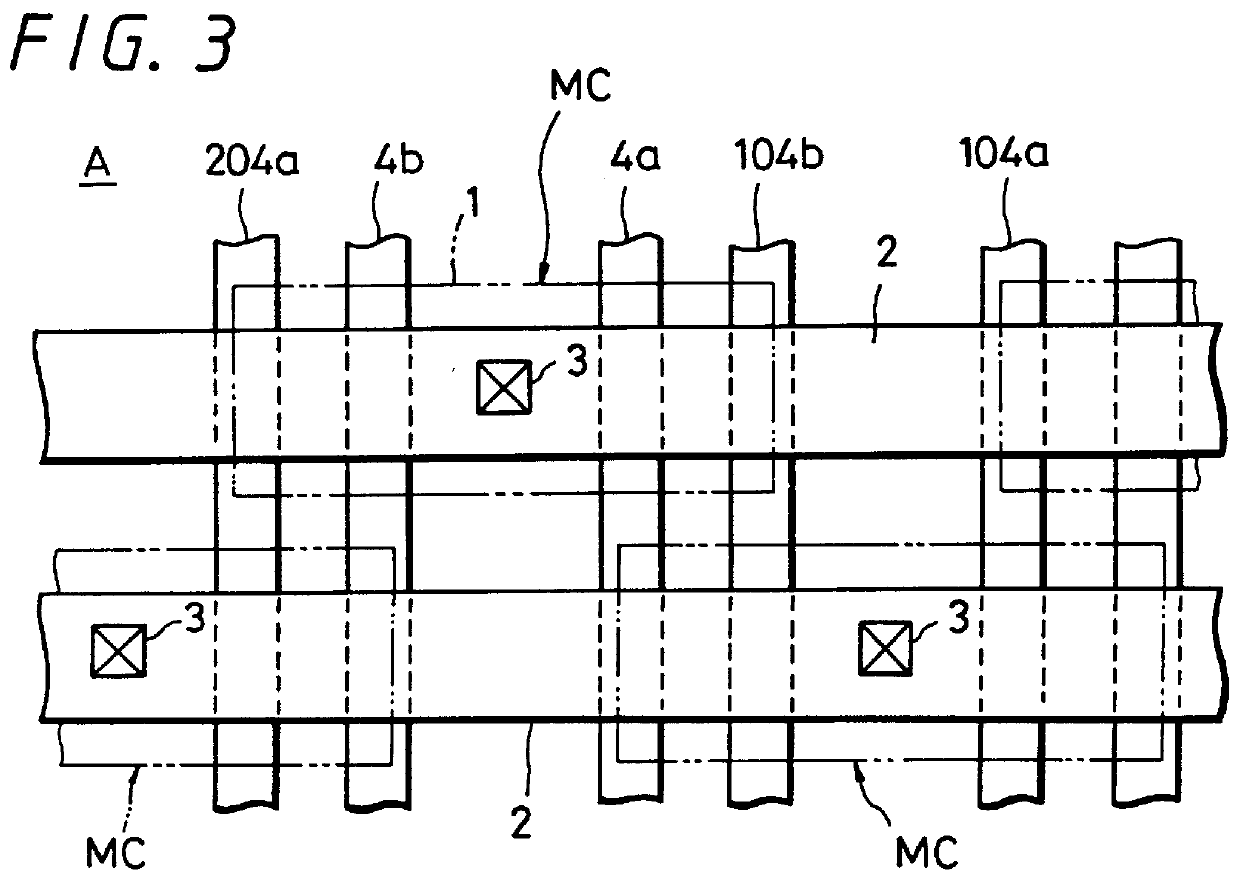
FIG. 2 shows a sectional view of a main portion of a semiconductor memory device A, particularly, a dynamic random access memory (DRAM) according to the first embodiment of the present invention, and FIG. 3 is a plan view thereof.

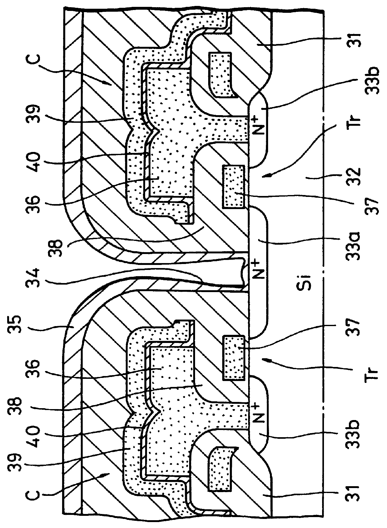
Referring initially to FIG. 3, it will be seen that the memory device A has formed at the central portion of an element forming region 1 encircled by an insulating layer formed of SiO.sub.2 or the like a contact portion 3 for a bit line 2 extending in the lateral direction. Two word lines 4a and 4b are symmetrically formed at left and right sides of the contact portion 3 so as to extend in the vertical direction. As shown in FIG. 2, one electrode 7a formed of a polycrystalline silicon layer so as to become an accumulation node (hereinafter referred to as an accumulation node electrode 7a) is formed through an insulating layer 6 under a switching element Tr1 composed of one word ...


PUM


Abstract

In a dynamic random access memory (DRAM), a step produced by forming a stacked capacitor can be prevented from being produced and increased, thereby facilitating the patterning of an upper layer (wiring, etc.). Further, the pattern layout can be made with freedom and the DRAM itself can be highly integrated. This dynamic random access memory is constructed such that stacked capacitors (C1), (C2) composed of accumulation node electrodes (7a), (7b), a dielectric layer (8) and a sub-plate electrode (9) are formed on the under layers of a switching element (Tr1) composed of a word line (4a) and two source-drain regions (5a), (5b) and a switching element (Tr2) composed of a word line (4b) and two source-drain regions (5a), (5c).

Description

1. Field of the InventionThe present invention generally relates to dynamic random access memories and, more particularly, is directed to a dynamic random access memory in which a stacked capacitor for charge accumulation is connected to a switching element.2. Description of the Prior ArtRecently, a stacked capacitor cell having a capacitor of a stacked type structure for storing informations has been utilized in order to keep a capacitance as semiconductor memories such as a dynamic random access memory (DRAM) or the like are highly integrated. This type of semiconductor memory is reported in international electron devices meeting held on Dec. 11, 1988, pp.596-599.As shown in FIG. 1, in a conventional semiconductor memory having a stacked capacitor, an impurity diffusion layer 33 of a switching element Tr is formed to face the surface of a silicon substrate 32 on which a field insulating layer 31 is formed. One source-drain region 33a of the impurity diffusion region 33 is connecte...

Claims


Application Information

Patent Timeline
IPC IPC(8): H01L21/02H01L29/66H01L21/70H01L27/12H01L21/84H01L21/8242H01L29/92H01L27/108H01L27/04H01L21/822H01L27/10
CPCH01L21/84H01L27/1082H01L28/40H01L27/10873H01L27/1203H01L27/10858H10B12/33H10B12/036H10B12/05H01L27/10
Inventor NISHIHARA, TOSHIYUKI
Owner SONY CORP
Why Eureka
Try Eureka