Liquid crystal display with sub-pixel electrodes, and control capacitor electrodes forming control capacitors

Inactive Publication Date: 2000-06-20
SEIKO EPSON CORP
View PDF14 Cites 58 Cited by
  • Summary
  • Abstract
  • Description
  • Claims
  • Application Information

AI Technical Summary

Problems solved by technology

However, in this method, there are various problems, such as that the process becomes complicated, and that reproducibility is not good.
However, in this background technology, in order to form the control capacitor (control capacity) and an additional capacitor, it is necessary to add processes such as a special electrode forming process, a dielectric film (insulating layer) forming process, and the like, which create problems, such as process lengtheni

Method used


Image

  • Liquid crystal display with sub-pixel electrodes, and control capacitor electrodes forming control capacitors
  • Liquid crystal display with sub-pixel electrodes, and control capacitor electrodes forming control capacitors
  • Liquid crystal display with sub-pixel electrodes, and control capacitor electrodes forming control capacitors

Examples


first embodiment

1. The First Embodiment

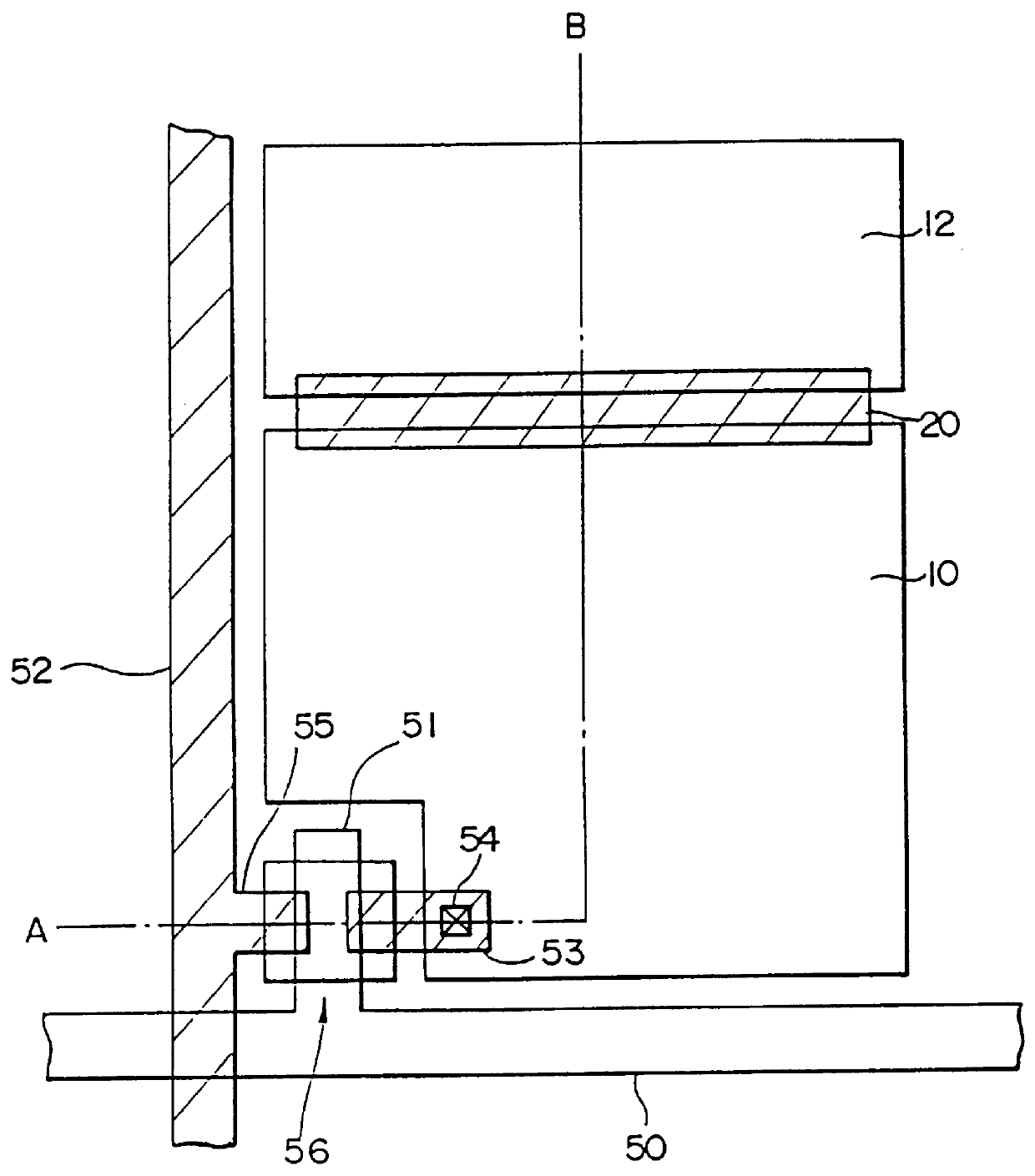
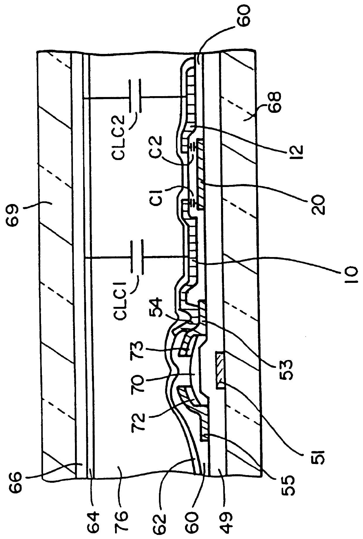
FIG. 1 shows a top view of the structure of the liquid crystal display element, related to the first embodiment, and FIG. 2 shows a cross section of A-B in FIG. 1.

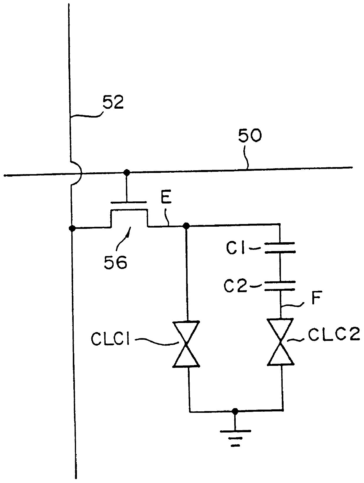
As shown in FIG. 1 and FIG. 2, this liquid crystal display element includes a thin film transistor (called TFT hereafter) 56, and a pixel electrode divided into first and second sub-pixel electrodes 10 and 12; it drives, by means of the pixel electrode, a liquid crystal layer 76 which is sealed by an opposing electrode 66. The TFT 56 includes a gate electrode 51, a source electrode 53, a drain electrode 55, an intrinsic silicon film 70, and n-type silicon films (ohmic layers) 72 and 73. The first sub-pixel electrode 10 is connected to the source electrode 53 through a contact 54, and the gate electrode 51 and the drain electrode 55 are connected to a scan line 50 and a signal line 52, respectively. The liquid crystal panel (liquid crystal device) is composed by positioning a plurality of the scan lin...

second embodiment

2. The Second Embodiment

FIG. 8 shows a top view of the structure of a liquid crystal display element related to the second embodiment, and FIG. 9 is a cross section of A-B in FIG. 8.

A difference from the first embodiment is the point in which a second control capacitor electrode 22 and a third sub-pixel electrode 14 are provided, and where control capacitors C3 and C4 are formed. As a result, an equivalent circuit diagram of the second embodiment becomes as shown in FIG. 10. Given a voltage of a terminal E as VE, this value VE, the voltage VF of the terminal F, and the voltage VD of the terminal G can be differentiated. Because of this, the light transmission rate of the liquid crystal layer in areas CLC1, CLC2, and CLC3, can be differentiated, and thus, the visual angle characteristics of these liquid crystal layers can be differentiated. Then, by these different visual angle characteristics being interpolated with each other, the visual angle characteristics of the entire body of ...

third embodiment

3. The Third Embodiment

FIG. 11 is a top view of the structure of a liquid crystal display element related to the third embodiment, and FIG. 12 shows a cross section of A-B in FIG. 11.

The difference from the first embodiment is the point concerning the formation of a holding capacitor CS between a scan line 40 connected to an adjacent TFT 46, and the second sub-pixel electrode 12. By having the holding capacitor CS formed, the problem of a decrease in the voltage caused by a voltage leak when the TFT 56 is off, can be solved, as is clear from the equivalent circuit diagram in FIG. 13. In that case, it is desirable if the scan line 40 which overlaps the second sub-pixel electrode 12 is a previously selected scan line (a scan line selected immediately before the scan line 50). That is, using FIG. 11 as an example, selected voltage is applied in the order of the scan lines 40 and 50. In such a way, fluctuations in voltage of the sub-pixel electrode 12, which originates in an application...


PUM


Abstract

PCT No. PCT/JP96/01652 Sec. 371 Date Mar. 27, 1997 Sec. 102(e) Date Mar. 27, 1997 PCT Filed Jun. 17, 1996 PCT Pub. No. WO97/00463 PCT Pub. Date Jan. 3, 1997A liquid crystal display element, a manufacturing method(s) thereof, and electronic devices (utilizing this element) which can improve, through a simple process, the visual angle characteristics, and the like, of liquid crystal panels is provided. A first control capacitor electrode (20) is included, provided below first and second sub-pixel electrodes (10, 12) and a protective insulating film (60). Also, control capacitors C1 and C2 are formed by the first and second sub-pixel electrodes (10, 12), and the first control capacitor electrode (20), through the protective insulating film (60). The visual angle characteristics of the liquid crystal panels are improved by the provision of the control capacitors C1 and C2. An increase in processes can be prevented, because the first control capacitor electrode (20) can be formed by a material identical to that of the source electrode. Moreover, the surface area of the control capacitor electrode can be miniaturized, and the aperture rate, and the like, can be improved, as a result of being able to make the protective insulating film (60) even thinner than the gate insulating film (49).

Description

1. Field of the InventionThe present invention relates to a liquid crystal display element in which pixel electrodes are divided into a multiple number of sub-pixel electrodes, a manufacturing method(s) thereof, and electronic devices (employing this element).2. Technical BackgroundAs described in Flat Panel Display 1994, in the article "The use of mass-produced panels using wide angle technology TFT for wide visual fields, as is required to make the leap to large size devices, is beginning to be seen in large size devices," (Dec. 10, 1993, Nikkei BP Company Publishing, page 166) various kinds of methods have been tested regarding wide angle visual field technology for liquid crystal panels. As representative of these methods, methods such as (1) a method for controlling liquid crystal orientation by techniques such as a rubbing process, and (2) a method for controlling voltage applied to liquid crystal molecules, utilizing a control capacitor, have been known.The above method (1) e...

Claims


Application Information

Patent Timeline
IPC IPC(8): G02F1/13G02F1/1362G02F1/1343
CPCG02F1/136213G02F2001/134345G02F1/134345G02F1/1343G02F1/136
Inventor SATOU, TAKASHI
Owner SEIKO EPSON CORP
Why Eureka
Try Eureka