Robust interconnect structure

a robust, copper interconnect technology, applied in the direction of electrical equipment, semiconductor devices, semiconductor/solid-state device details, etc., can solve the problems of failures during rework and burn-in operations, silicon nitride not showing strong adhesion to copper surfaces, and the nitride-to-copper interface is susceptible to delamination, so as to improve the structural integrity of copper interconnects

Inactive Publication Date: 2000-10-17
INVENSAS CORP
View PDF6 Cites 80 Cited by
  • Summary
  • Abstract
  • Description
  • Claims
  • Application Information

AI Technical Summary

Benefits of technology

The present invention provides for improved structural integrity of copper interconnects including C4 over copper BEOL. The present invention provides for interconnect that is robust to mechanical stresses.

Problems solved by technology

However, silicon nitride does not exhibit strong adhesion to copper surfaces despite various adhesion treatments.
Accordingly, the silicon nitride-to-copper interface is susceptible to delamination under conditions of mechanical loading.
Failures arose during rework and burn-in operations due to the inherently relatively weak adhesion of the overlying silicon nitride cap to the copper.

Method used


Image

  • Robust interconnect structure
  • Robust interconnect structure

Examples


Embodiment Construction

In order to facilitate an understanding of the present invention, reference will be made to the drawings.

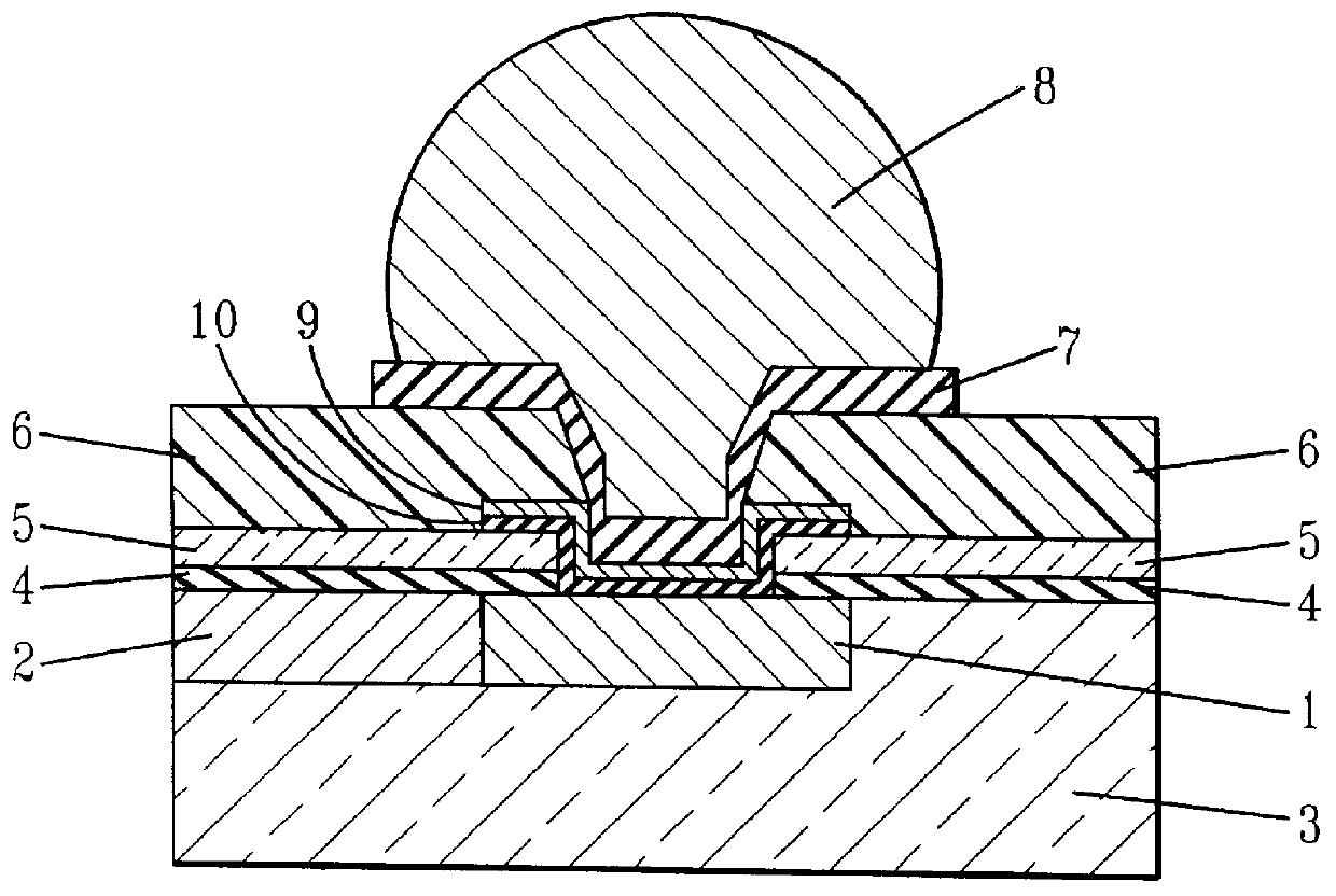
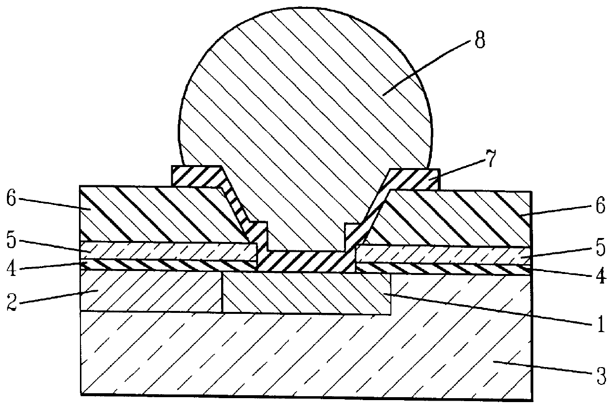
In particular, FIG. 1 is a schematic diagram of a prior art C4 over Cu Back End of the Line (BEOL) structure wherein a copper pad 1 is connected to a conductor 2 and within an opening or via through an isolation region 3. Typically, a barrier or liner layer (not shown) will be present on the sides and bottom of the copper pad, between the conductor 2 and isolation region 3.

The isolation region 3 is typically silicon dioxide. The copper layer is typically about 0.3 to about 2 .mu.m thick and more typically about 0.5 to about 1.2 .mu.m thick.

A capping layer 4 such as silicon nitride is provided above the copper layer. In the case of silicon nitride, it can be deposited by a well known plasma enhanced chemical vapor deposition process (PECVD). Such process involves introducing a silicon-bearing gas species such as silane and a nitrogen-bearing gas species such as ammonia and / or nitr...


PUM

PropertyMeasurementUnit
thickaaaaaaaaaa
thickaaaaaaaaaa
thickaaaaaaaaaa

Abstract

A structure comprising a layer of copper, a barrier layer, a layer of AlCu, and a pad-limiting layer, wherein the layer of AlCu and barrier layer are interposed between the layer of copper and pad-limiting layer.

Description

TECHNICALThe present invention relates to metal interconnects and more particularly to a robust copper interconnect structure. The present invention finds particular applicability for VLSI and ULSI copper interconnects especially for packaging.BACKGROUND OF INVENTIONInterest in using copper as interconnects in semiconductor devices continues to increase since it possesses a lower resistivity and a reduced susceptibility to electromigration failure as compare to the more traditional aluminum or aluminum alloy interconnects.However, since copper has a tendency when used in interconnect metallurgy to diffuse into surrounding dielectric materials such as silicon dioxide, capping of the copper is essential. The capping inhibits this diffusion. One widely suggested method of capping includes employing a conductive barrier layer along the sidewalls and bottom surface of a copper interconnect. Typical of such barrier layers is tantalum or titanium. Capping of the upper surface of a copper i...

Claims


Application Information

Patent Timeline
Patent Type & Authority Patents(United States)
IPC IPC(8): H01L21/02H01L21/60H01L23/485H01L23/48H01L21/3205H01L23/52
CPCH01L24/05H01L24/11H01L24/13H01L2924/01007H01L2924/0002H01L2924/01014H01L2924/01022H01L2924/01029H01L2924/01033H01L2924/0105H01L2924/01052H01L2924/01073H01L2924/01074H01L2924/01078H01L2924/01079H01L2924/01082H01L2924/014H01L2924/04941H01L2924/04953H01L2924/05042H01L2924/14H01L2924/3025H01L2924/01013H01L2924/0001H01L2224/13007H01L23/3192H01L2224/05027H01L2224/13111H01L2224/05572H01L2924/01084H01L2924/01024H01L2224/0401H01L2224/05022H01L2224/05647H01L2224/13099H01L2924/01006H01L2924/0102H01L2924/01023H01L2924/00014H01L2224/05552H01L23/485
Inventor EDELSTEIN, DANIEL CHARLESMCGAHAY, VINCENTNYE, III, HENRY A.OTTEY, BRIAN GEORGE REIDPRICE, WILLIAM H.
Owner INVENSAS CORP
Why Eureka
Try Eureka