Method for manufacturing capacitor of semiconductor device including thermal treatment to dielectric film under hydrogen atmosphere

a semiconductor device and dielectric film technology, applied in the direction of semiconductor devices, capacitors, electrical equipment, etc., can solve the problems of complex process, increased process cost, and variation of threshold voltag

Inactive Publication Date: 2000-10-24
SAMSUNG ELECTRONICS CO LTD
View PDF8 Cites 40 Cited by
  • Summary
  • Abstract
  • Description
  • Claims
  • Application Information

AI Technical Summary

Problems solved by technology

Also, when a capacitor having a three-dimensional structure is fabricated to increase the effective area of the capacitor, the process thereof is complicated and the cost for the process increases.
As another drawback, a silicon dangling bond effect occurs at the interface between a silicon and a silicon oxide film in a transistor of a semiconductor device.
The interface trap affects the height of a Schottkey barrier, thus causing variation of a threshold voltage.

Method used


Image

  • Method for manufacturing capacitor of semiconductor device including thermal treatment to dielectric film under hydrogen atmosphere
  • Method for manufacturing capacitor of semiconductor device including thermal treatment to dielectric film under hydrogen atmosphere
  • Method for manufacturing capacitor of semiconductor device including thermal treatment to dielectric film under hydrogen atmosphere

Examples


Embodiment Construction

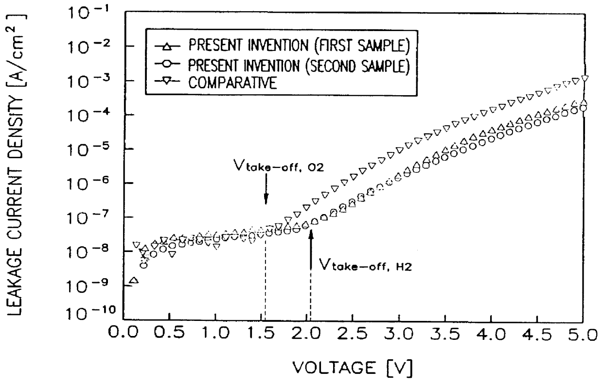
FIG. 3 is a graph illustrating the decreased leakage current characteristic of capacitors formed according to the present invention compared to capacitors formed using conventional methods.

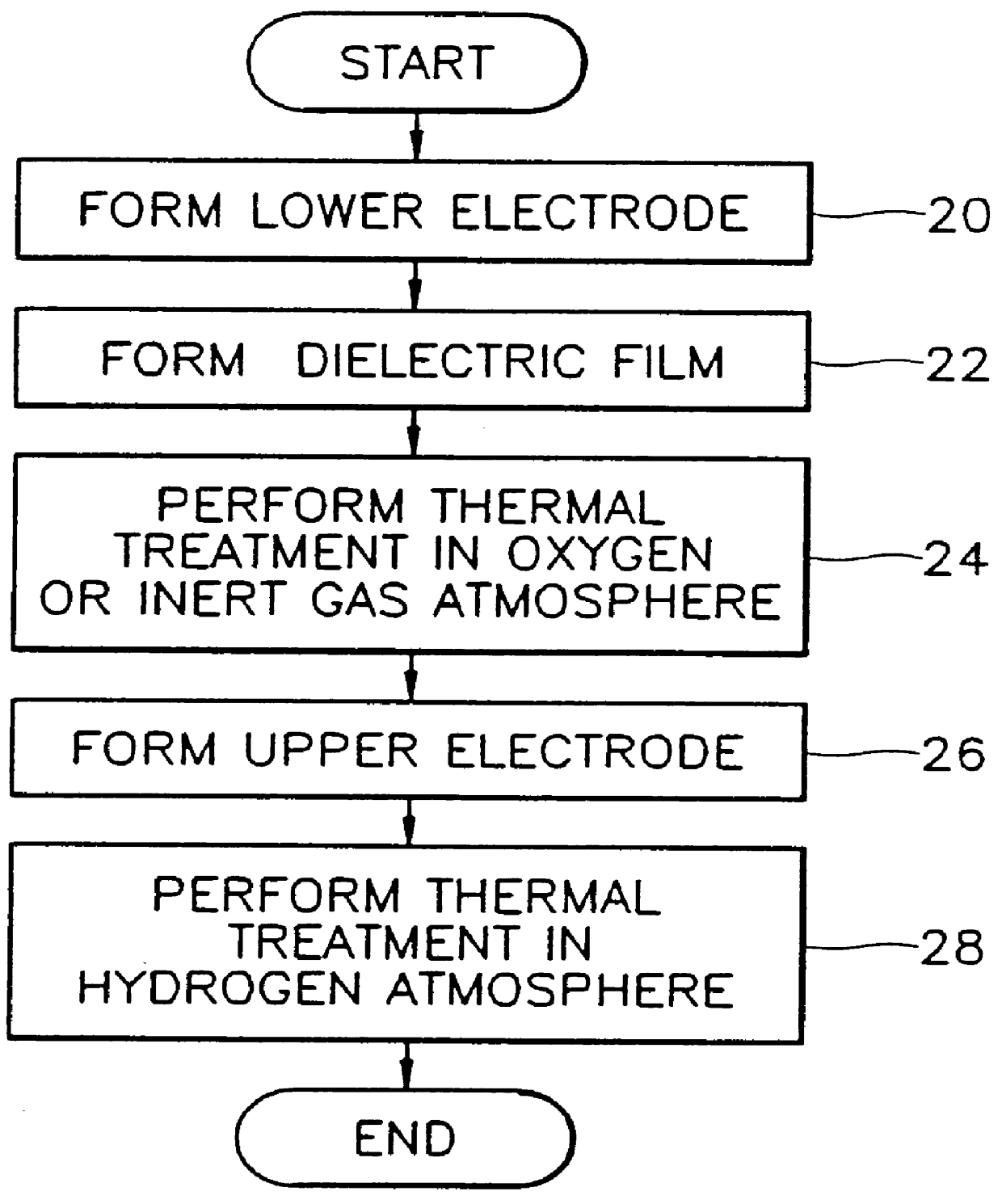
In order to obtain the results of FIG. 3, the capacitors of first and second samples (-.DELTA.-) and (-.smallcircle.-) were fabricated using the method described above with reference to FIGS. 1 and 2, respectively. Also, the capacitor of a comparative sample (-.gradient.-) was fabricated using conventional methods. Then, the density of leakage current at each operation voltage was measured.

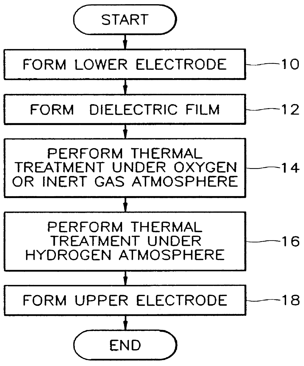
The first sample was fabricated as follows. First, a lower electrode of impurity-doped polysilicon is formed on a semiconductor substrate. A dielectric film of tantalum oxide (Ta.sub.2 O.sub.5) was formed on the lower electrode. An oxygen-atmosphere thermal treatment was performed on the resultant structure on which the dielectric film was formed, at a temperature of 800.degree. C. using wet O.sub.2 for 30 minut...


PUM

PropertyMeasurementUnit
temperatureaaaaaaaaaa

Abstract

A capacitor fabricating method for a semiconductor device where a dielectric film is thermally treated under hydrogen atmosphere to improve interface characteristics between the dielectric film and an electrode. In the method, a lower electrode is formed on a semiconductor substrate. A dielectric film is formed on the lower electrode. The dielectric film is thermally treated under hydrogen atmosphere. An upper electrode is formed on the dielectric film, thereby completing formation of the capacitor. The thermal treatment under the hydrogen atmosphere is performed at a temperature of 300 to 600 DEG C. using H2 gas or H2 plasma for 5 to 60 minutes. Thus, the density of an interface trap between the electrode and the dielectric film of the capacitor is reduced.

Description

1. Field of the InventionThe present invention relates to a semiconductor device fabricating method, and more particularly, to a method for fabricating a capacitor of a semiconductor device for reducing leakage current between a dielectric film and an electrode.2. Description of the Related ArtCapacitance (C) of a capacitor in a semiconductor device is expressed by the following Equation 1. ##EQU1##Here, .epsilon..sub.0 denotes permittivity in a free space, .di-elect cons..sub.r denotes a dielectric constant of the particular dielectric film used, A denotes an effective area of an electrode, and d denotes the thickness of the dielectric film. As can be seen from Equation 1, capacitance is increased by changing three variables, i.e., the dielectric constant of the dielectric film, the effective area of a capacitor, and the thickness of the dielectric film.Each of these methods for increasing the capacitance has its drawbacks. When a material having a large dielectric constant is used...

Claims


Application Information

Patent Timeline
Patent Type & Authority Patents(United States)
IPC IPC(8): H01L21/02H01L21/3105H01L21/314H01L21/316H01L29/12
CPCH01L21/3105H01L28/55H01L21/31691H01L21/02164H01L21/02183H01L21/02178H01L21/02186H01L21/0217H01L21/02197H01L29/12H01L21/0234
Inventor WON, SEOK-JUNNAM, KAB-JINPARK, YOUNG-WOOK
Owner SAMSUNG ELECTRONICS CO LTD
Why Eureka
Try Eureka