Semiconductor device and manufacturing method thereof

a technology of semiconductors and semiconductors, applied in the direction of semiconductor devices, electrical devices, transistors, etc., can solve the problems of irregular crystal structure on this interface, undesirable thin film thickness of 2 nm or less, and the thickness of the thin film equal or higher than 2 nm

Inactive Publication Date: 2000-10-31
KK TOSHIBA
View PDF4 Cites 17 Cited by
  • Summary
  • Abstract
  • Description
  • Claims
  • Application Information

AI Technical Summary

Problems solved by technology

The generation of this leakage current lets the electric charge accumulated in the charge storage capacitor section run into the n.sup.+ drain region 62 despite opening / closing of the access transistor and results in a malfunction.
In other words, growth faces presenting different face orientations collide one the other, causing the crystal structure irregularity on this interface.
It is undesirable that the thin film thickness be equal to or higher than 2 nm, because the ohmic contact between the conductor and the second semiconductor region will be inhibited.
Moreover, in respect of a process where a buried contact is formed by a self alignment process, a thin film thickness equal to or higher than 2 nm is undesirable, because this thin film will inhibit the diffusion.
It is undesirable that the thin film thickness be equal to or higher than 2 nm, because the ohmic contact between the conductor and the second semiconductor region will be inhibited.

Method used


Image

  • Semiconductor device and manufacturing method thereof
  • Semiconductor device and manufacturing method thereof
  • Semiconductor device and manufacturing method thereof

Examples


first embodiment

(First Embodiment)

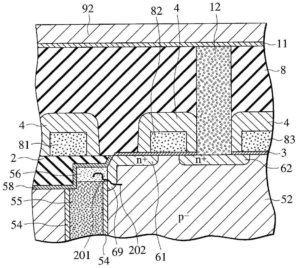
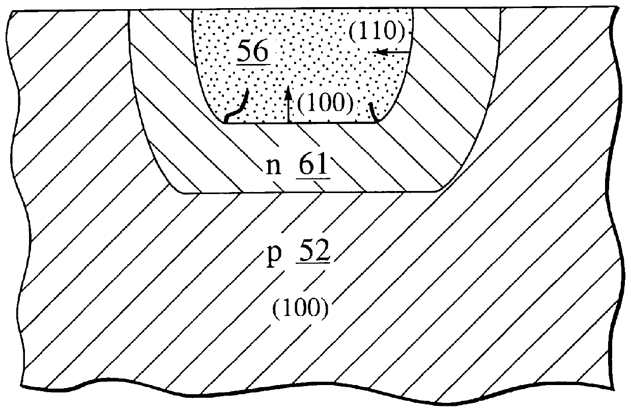
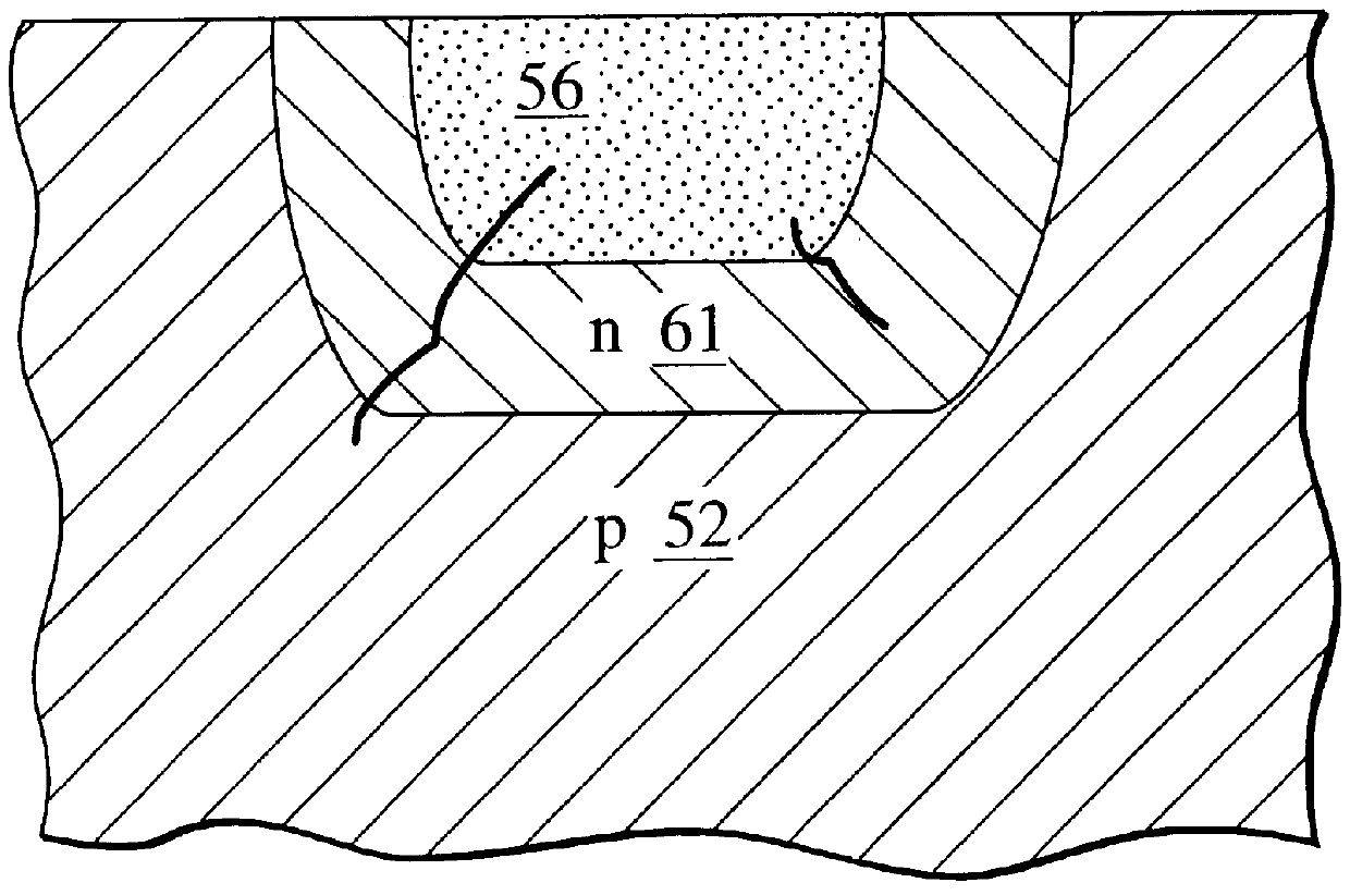
FIG. 3 is a cross section of a DRAM according to a first embodiment of the present invention. The DRAM according to the first embodiment of the present invention is composed by arranging a number of memory device element (memory cell) in the form of X-Y matrix. Each memory cell is composed of one access transistor and one charge storage capacitor section (capacitor section). FIG. 3 is a partial view showing one memory cell among them. A contact plug 12 disposed at the center of these two memory cells is connected to a bit line 92 extending to the left and to the right. At the left of the central contact plug 12, an access transistor composed of an n.sup.+ source region 61 and an n.sup.+ drain region 62 is disposed. The n.sup.+ silicon region including n.sup.+ source region 61 includes a buried contact 69. Moreover, at the left of the n.sup.+ source region 61, a charge storage capacitor section (trench capacitor section) 6 is situated, and n.sup.+ source region 61 a...

second embodiment

(Second Embodiment)

In the first embodiment, a trench type DRAM has been described, however, it is nothing but an illustrative example, and obviously, it can also be applied to stack type DRAM, fin type DRAM, or various other DRAMs. FIG. 9 is a schematic cross-section of a fin type DRAM according to the second embodiment of the present invention. In FIG. 9, there is an active region surrounded by an isolation region 2 formed by STI process or the like on the surface of a p type (100) silicon substrate 101. An n.sup.+ source region 61 and an n.sup.+ drain region 62 of an access transistor are disposed on this active region. The region between the n.sup.+ source region 61 and the n.sup.+ drain region 62 of the access transistor constitutes the channel region. Gate electrodes 86, 87, 88 of poly silicon or the like are formed on the upper portion of this channel region via a gate oxide film 3. The poly silicon electrodes 86, 87, 88 serve also as word lines, and extend in a direction orth...

third embodiment

(Third Embodiment)

The present invention is not limited to the memory device shown in the first or second embodiments. Nor, it is not limited to the MOS integrated circuit shown in the first or second embodiments. FIG. 11 is a cross section of a bipolar integrated circuit as a third embodiment of the present invention. This bipolar integrated circuit illustrates a part of TTL logic circuit as an example. In FIG. 11, an n.sup.+ buried layer 566 (buried collector region) is formed on a p type (100) silicon substrate 102, and an n well region (collector) 565 is formed on that n.sup.+ buried collector region 566. A p base region 563 and an n.sup.+ emitter region 564 are formed on the collector region 565. A p.sup.+ base contact region 569 is formed on a part of the surface of the p base region 563. On the other hand, an isolation region 2 is formed by STI process or the like on the n collector region 565. An interlayer insulation film 8 is formed on the n collector region 565, the p.sup....


PUM

PropertyMeasurementUnit
thicknessaaaaaaaaaa
temperatureaaaaaaaaaa
thicknessaaaaaaaaaa

Abstract

A semiconductor device provided with a thin film of 0.1 nm to 2 nm in thickness, having a crystal structure different from that of a conductor and a semiconductor region, between the conductor and the semiconductor region. When the semiconductor region is made of single crystal silicon and the conductor region is made of amorphous silicon or poly silicon, the oxygen surface concentration of the thin film is equal to or higher than 1x1015 cm-2 and equal to or lower than 4x1015 cm-2 in one case, that of oxygen is equal to or higher than 1x1015 cm-2 and equal to or lower than 2x1015 cm-2 and that of nitrogen is equal to or higher than 1x1015 cm-2 and equal to or lower than 4x1015 cm-2 in the other case. The presence of the thin film prevents the epitaxial growth from starting from the interface between the conductor and the semiconductor region and reduces the crystal defect formation and growth near the interface.

Description

1. Filed of the InventionThe present invention relates to a semiconductor device requiring a high level integration such as dynamic RAMs (DRAMs) and a manufacturing method thereof, and more particularly, a semiconductor device having a structure for realizing a good electric connection between an buried conductor and a semiconductor region and a manufacturing method thereof.2. Description of the Related ArtIn recent years, semiconductor integrated circuits are integrated in larger and larger scale and, more particularly, DRAMs having a high integration by giga bits are demanded. According to such higher integration of semiconductors, the semiconductor devices are developed into three-dimensional structure from two-dimensional structure as before and a technology for obtaining a contact region substantially equal to or higher than the conventional one are adopted there to within a projective region smaller in two-dimensional plane than before. Usually, the DRAM memory cell of one tra...

Claims


Application Information

Patent Timeline
Patent Type & Authority Patents(United States)
IPC IPC(8): H01L21/70H01L21/8242H01L27/108H01L21/28H01L21/768H01L21/8246H01L27/105H01L29/43
CPCH01L27/10867H01L27/10852H10B12/0385H10B12/033H10B12/00
Inventor SUGIURA, SOICHIWATANOBE, HISASHI
Owner KK TOSHIBA
Why Eureka
Try Eureka