Laser assembly platform with silicon base

a silicon base and assembly platform technology, applied in the field of lasers, can solve the problems of poor thermal conductivity, poor heat dissipation performance, and inability to overcome expensive or impossible problems

Inactive Publication Date: 2001-01-23
PHOTERA TECH
View PDF11 Cites 28 Cited by
  • Summary
  • Abstract
  • Description
  • Claims
  • Application Information

AI Technical Summary

Problems solved by technology

However, the large coefficient of thermal expansion for these metals renders them unsuitable for precision placement of optical components thereon, because even a small relative movement between optical components can drastically degrade performance of the laser and optical processing functions.
However, these materials are generally poor thermal conductors, which lead to heat dissipation problems that can be expensive or impossible to overcome.
When metals such as copper and alloys such as invar are used as optical benches, each optical bench is machined individually, leading to inconsistencies between parts as well as adding significant cost.
Furthermore, the inability of machining processes to achieve close tolerances requires substantial additional work (i.e. additional cost) to assemble a complete laser assembly.
Invar particularly is very difficult to machine.
However, three dimensional features in metals cannot be etched with sufficient precision, leaving machining as the only practical alternative for forming an optical bench of metals and alloys.
Lasers assemblies have been manufactured by hand by gluing free-standing optical components on optical benches in an exacting and laborious process For example, a skilled technician mounts each individual component on the optical benches, aligns each as it is glued into place, and then holds it in place for the length of time necessary to obtain a bond.
Due to the extremely narrow tolerances of optical systems, it can be difficult and time-consuming to achieve such tolerances

Method used


Image

  • Laser assembly platform with silicon base
  • Laser assembly platform with silicon base
  • Laser assembly platform with silicon base

Examples


Embodiment Construction

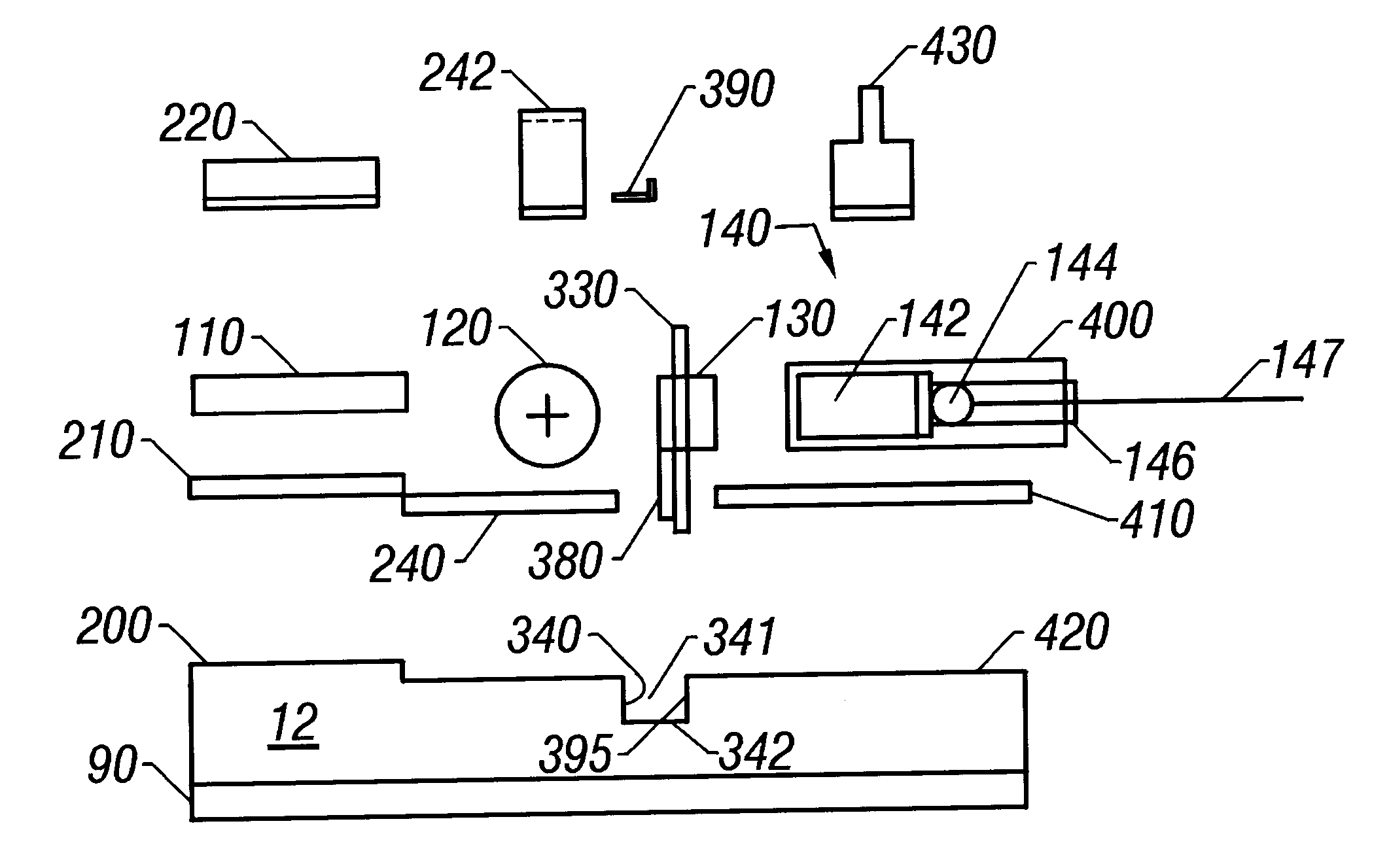
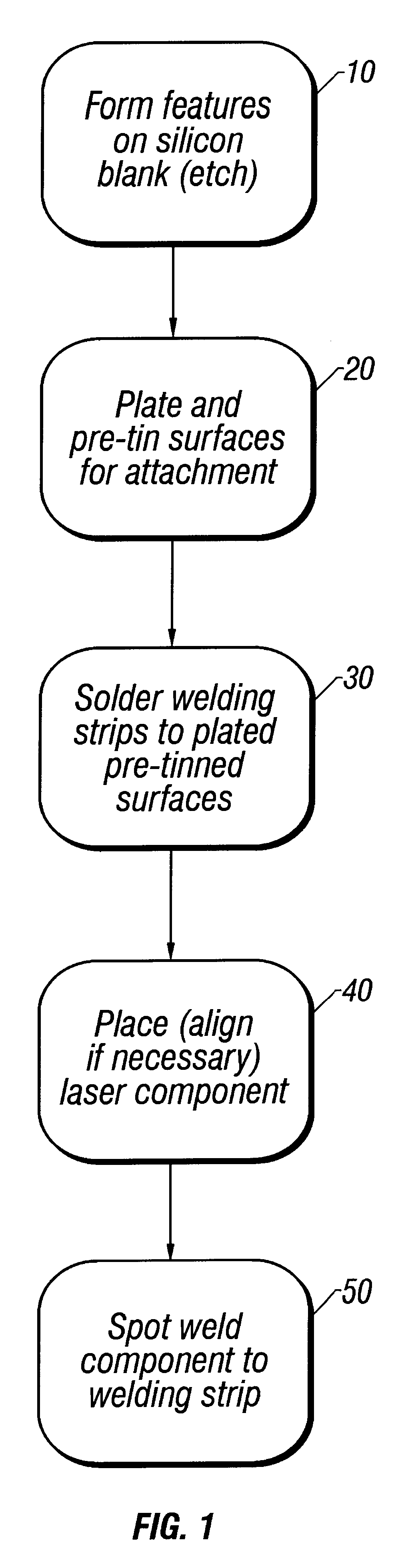
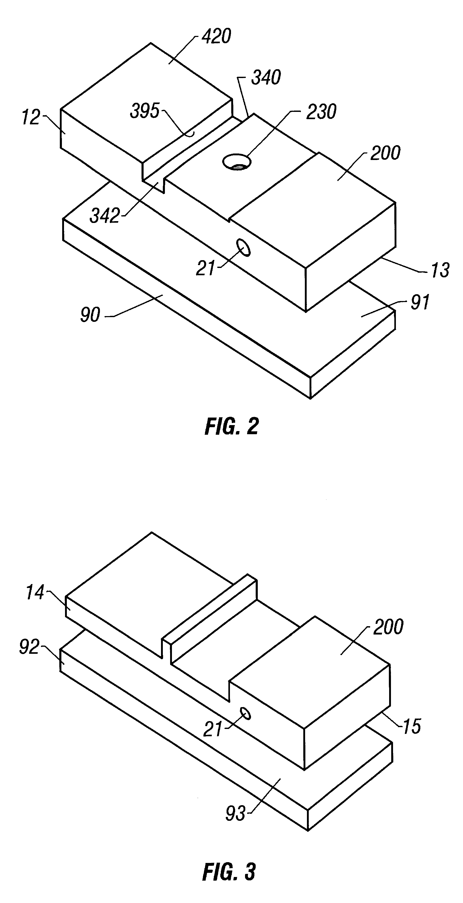
Specific embodiments of the invention are described below with reference to the Figures, in which like numbers represent the same or similar elements.

An assembly process and platform including a silicon optical bench or base is described. The elements of a laser such as a DPSSL are mounted on the silicon base to form a laser assembly . The process can provide a low cost, reliable method for manufacturing a laser with a silicon base. Generally, the silicon base is precisely formed as a monolithic structure with features that define the position of the optical components of the laser assembly. As a result, the manufacturing process is simplified and only a small amount of hand adjustment is required during assembly.

Use of silicon for the base can be advantageous because it is readily available, it has good thermal conductivity and it has a low coefficient of thermal expansion. Single-crystal silicon is particularly useful, although polycrystalline silicon could be used for some applic...


PUM


Abstract

A laser assembly including a silicon base and method are provided for assembling lasers on a platform in a reliable, low cost process that is suitable for high volume production. The platform can be a monolithic silicon base which has high thermal conductivity, a low coefficient of thermal expansion, and whose features can be formed with close tolerances in a low cost, reliable manner. Materials with similar coefficients of thermal expansion are used in order to maintain alignment during unexpected heating and cooling. Furthermore, a method is described that substantially eliminates the need for adhesives to bond laser components to a platform. The resultant laser can be very robust, stable, and can provide reliable operation over extended time periods.

Description

1. Field of the InventionThe present invention relates to lasers, and particularly to manufacturing lasers using a monolithic platform that has a silicon base.2. Description of Related ArtOne important type of laser is a diode-pumped solid-state laser ("DPSSL"), which includes a solid-state gain medium pumped by optical radiation from a laser diode. Diode-pumped solid-state lasers can be useful in a wide variety of applications including laser display systems, optical data storage systems, medical instrumentation, and telecommunications. For small to moderate levels of optical power, one particularly useful diode-pumped solid-state laser is a microlaser, which comprises a short element (i.e. less than about five mm) of solid-state gain medium positioned in a resonant cavity. The pump beam is supplied by a semiconductor diode laser, which pumps the solid-state gain medium to provide energy to support laser operation within the resonant cavity. Two opposing reflective surfaces define ...

Claims


Application Information

Patent Timeline
IPC IPC(8): H01S5/022H01S5/00H01S3/16H01S3/0941H01S5/02
CPCH01S3/025H01S5/02252H01S3/005H01S3/0064H01S3/0627H01S3/09415H01S5/02326
Inventor JING, XINGLIANGLEILABADY, PEDRAM A.
Owner PHOTERA TECH
Why Eureka
Try Eureka