Switched backgate bias for FET

a backgate bias and fet technology, applied in the field of semiconductor circuits and mosdrams, can solve the problems of significant delay in switching, subthreshold leakage, and current flowing between source and drain, and achieve the effect of reducing the number of transistors, and improving the efficiency of switching

Inactive Publication Date: 2001-05-15
RENESAS ELECTRONICS CORP
View PDF15 Cites 143 Cited by
  • Summary
  • Abstract
  • Description
  • Claims
  • Application Information

AI Technical Summary

Problems solved by technology

When the threshold voltage is reduced or the channel length is made shorter for MOS-FETs to achieve higher switching speeds, there arises the problem that the drain and source depletion layers can easily be connected together, causing a punch-through situation where current flows between source and drain even when the channel is not formed.
This, however, causes the problem that the subthreshold leakage increases.
When this happens, when switching from standby to active state, a significant delay may occur in the switching because of such changes in the potential of the secondary power supply line V.sub.CC1 or of the secondary ground line V.sub.SS1, and in the worst case, the logic may change.
In this configuration, however, subthreshold current flows into the word drivers in the standby state; this becomes a problem in realizing low-power dissipation circuit design.
The word driver configuration shown in FIG. 5, however, has the problem that the rising of the selected word line delays since the source voltage of the pMOS-FET Q61 need to be raised from a slightly dropped level to the power source potential when switching from the standby state to the active state.

Method used


Image

  • Switched backgate bias for FET
  • Switched backgate bias for FET
  • Switched backgate bias for FET

Examples


first embodiment

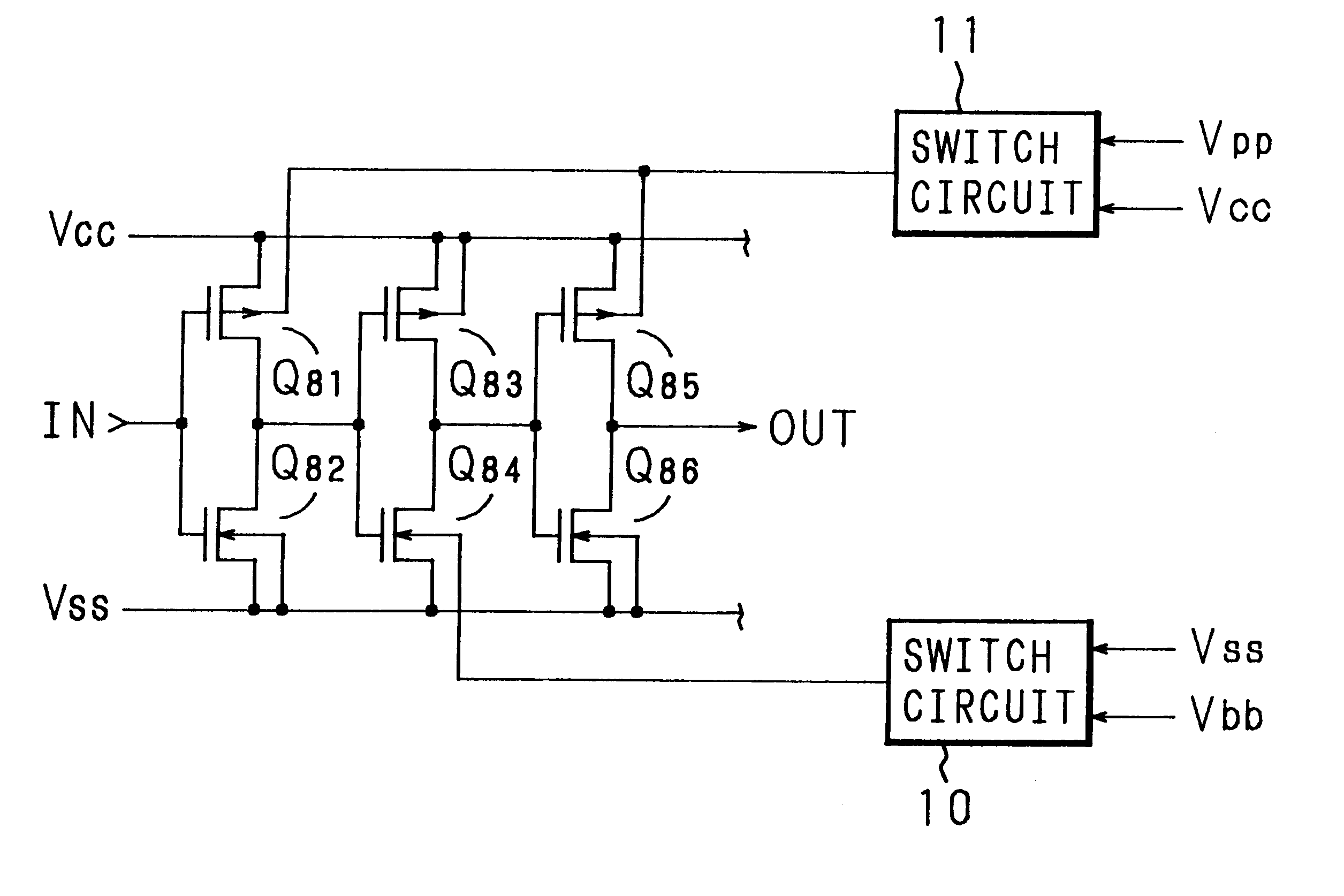
FIG. 6 is a circuit diagram of a complementary MOS inverter, showing a logic circuit constituting the semiconductor circuit according to the present invention. Power source potential V.sub.CC is applied to the source of an FET Q1, and ground potential V.sub.SS is applied to the source of an FET Q2. The gates of the FET Q1 and FET Q2 are connected to form an input node IN, and their drains are connected to form an output node OUT. The backgate of the FET Q2 is connected to a switch circuit 10 which switches the ground potential V.sub.SS (=0 V) and potential V.sub.bb (<0 V) lower than the ground potential V.sub.SS, and the backgate of the FET Q1 is connected to a switch circuit 11 which switches the power source potential V.sub.cc and potential V.sub.PP higher than the power source potential V.sub.cc.

Here, the FET Q1 and FET Q2 are designed so that, when the potential V.sub.PP higher than the power source potential V.sub.CC and the potential V.sub.bb lower than the ground potential V....

embodiment 2

FIGS. 10 and 11 are block diagrams showing the configuration of a MOS-DRAM according to a second embodiment of the present invention. An external row address signal is inputted via input terminals ex. A.sub.0 -ex. A.sub.n into an input buffer 26, latched into a latch circuit 27, and then fed into a row decoder 29 through a buffer gate array 39. The row decoder 29 selects an appropriate word line WL.sub.0 -WL.sub.m, and the selected word line WL.sub.0 -WL.sub.m is driven by a word driver 30 to access the intended memory cell 57 connected to that word line in a memory cell array 33.

The contents of the accessed memory cell 57 are outputted to a bit lines BL.sub.0 -BL.sub.k and amplified by sense amplifiers SA.sub.0 -SA.sub.k, while at the same time the same contents are rewritten into the memory cell 57.

On the other hand, an external column address signal, inputted via input terminals, an input buffer, a latch circuit, and a buffer gate array, is fed into a column decoder 31, then sele...

embodiment 3

FIG. 14 is a block diagram showing the configuration of a memory cell according to a third embodiment of the present invention. One electrode of a capacitor 50 is connected to the source of an nMOS-FET 37, and the gate and drain of the nMOS-FET 37 are connected to a word line WL and a bit line BL, respectively. The other electrode of the capacitor 50 is connected to a cell plate 51. Connected to the backgate of the FET 37 is a switch circuit 36 that switches potential V.sub.bb2 supplied from a voltage supply means 48b and potential V.sub.bb1 supplied from a voltage supply means 48a (where V.sub.bb1

FIG. 15 is a circuit diagram showing a configurational example of the switch circuit 36, which is substantially same as the circuit diagram of the switch circuit 10 shown in FIG. 7. In FIG. 15, the voltage supply means 48a, potential V.sub.bb2 from the voltage supply means 48b, clock signal generator 49, external RAS (row address strobe) signal (external row select signal) ex....


PUM


Abstract

A semiconductor circuit or a MOS-DRAM wherein converting means is provided that converts substrate potential or body bias potential between two values for MOS-FETs in a logic circuit, memory cells, and operating circuit of the MOS-DRAM, thereby raising the threshold voltage of the MOS-FETs when in the standby state and lowering it when in active state. The converting means includes a level shift circuit and a switch circuit. The substrate potential or body bias potential is controlled only of the MOS-FETs which are nonconducting in the standby state; this configuration achieves a reduction in power consumption associated with the potential switching. Furthermore, in a structure where MOS-FETs of the same conductivity type are formed adjacent to each other, MOS-FETs of SOI structure are preferable for better results.

Description

1. Field of the InventionThe present invention relates to improvements in semiconductor circuits and MOS-DRAMs, which use fabricated from MOS-FETs.2. Description of Related ArtFIG. 1 is a circuit diagram showing a complementary MOS inverter used in a conventional semiconductor circuit. Power source potential V.sub.CC is applied to the source and backgate (substrate) of a pMOS-FET Q1, and ground potential VsS is applied to the source and backgate of an nMOS-FET Q2. The gates of the FETs Q1 and Q2 are connected to form an input node IN, and their drains are connected to form an output node OUT.The operation of the thus configured complementary MOS inverter will be described below.When a logic signal of high level (power source potential V.sub.CC) is inputted to the input node IN, the FET Q1 is turned off and the FET Q2 is turned on, so that a logic signal of low level (ground potential V.sub.SS =0 V) is outputted from the output node OUT through the FET Q2.Conversely, when a logic sig...

Claims


Application Information

Patent Timeline
Patent Type & Authority Patents(United States)
IPC IPC(8): H01L27/02H01L27/12H03K19/00
CPCH01L27/0218H01L27/1203H03K19/0016H03K2217/0018G11C11/407
Inventor ARIMOTO, KAZUTAMITSUKUDE, MASAKI
Owner RENESAS ELECTRONICS CORP
Why Eureka
Try Eureka