Direct deposit thin film single/multi chip module

a single/multi-chip module and direct deposit technology, applied in the direction of resistive material coating, cable/conductor manufacturing, printed circuit non-printed electric components association, etc., can solve the problems of increasing signal load capacitance, increasing single-chip modules (scms) and, especially, multi-chip modules (mcms), and impairing chip performan

Inactive Publication Date: 2001-07-17
INT BUSINESS MASCH CORP
View PDF12 Cites 26 Cited by
  • Summary
  • Abstract
  • Description
  • Claims
  • Application Information

AI Technical Summary

Problems solved by technology

Performance and signal density demands are forcing Single chip modules (SCMs) and, especially, multi-chip modules (MCMs) to become more and more complex.
However, increasing signal density, increases signal load capacitance and impairs chip performance.
Unfortunately, these TF processes adapted for making such a module are very expensive because they require a planar ceramic substrate surface.

Method used


Image

  • Direct deposit thin film single/multi chip module
  • Direct deposit thin film single/multi chip module
  • Direct deposit thin film single/multi chip module

Examples


Embodiment Construction

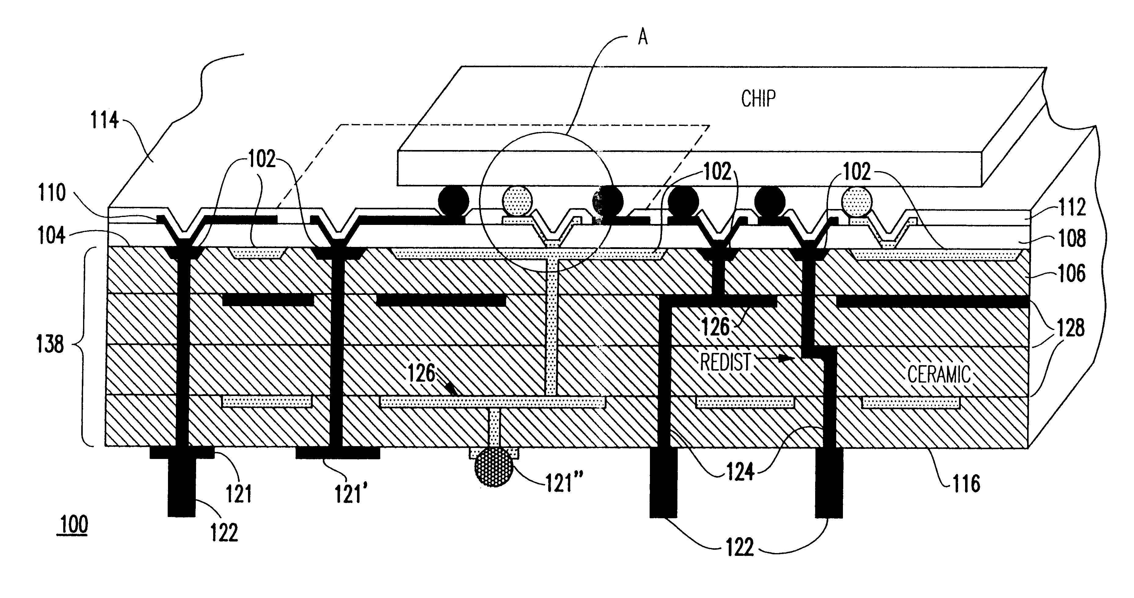
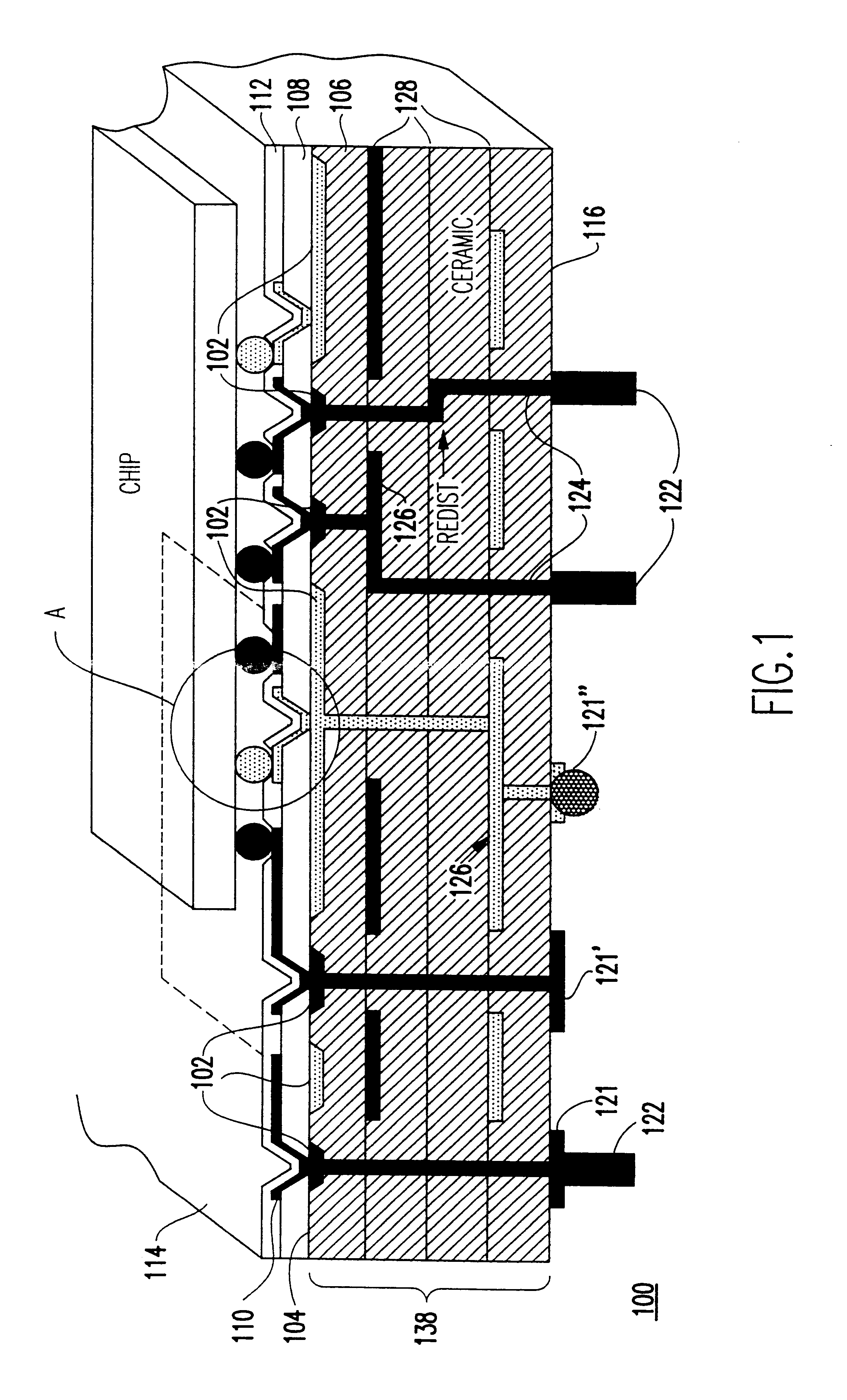
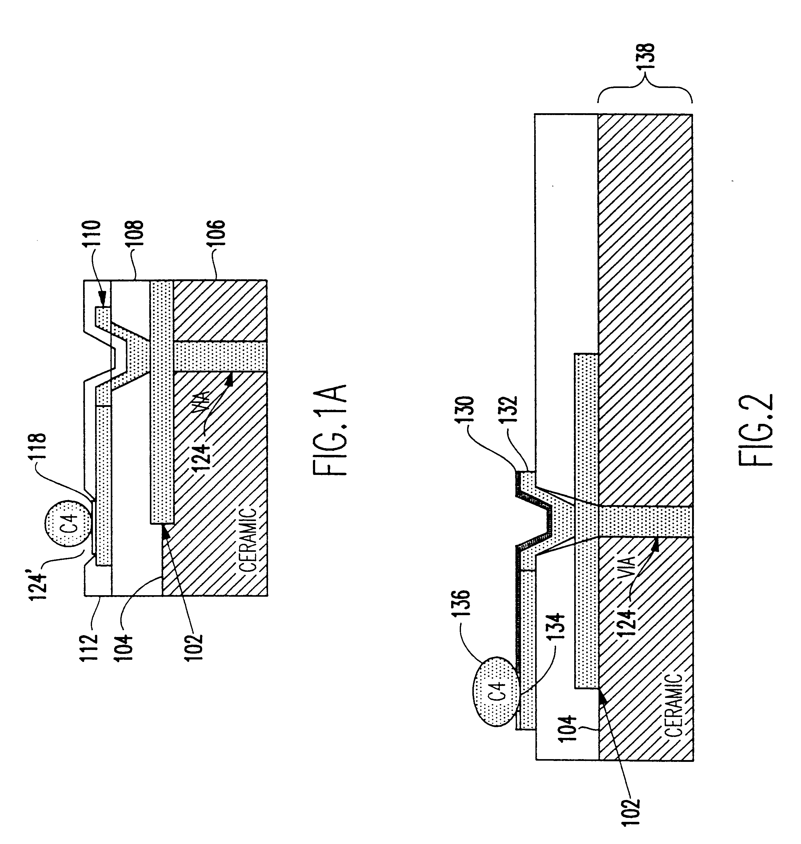
Referring now to the drawings, and more particularly to FIG. 1, there is a preferred embodiment ceramic carrier 100. The carrier includes a sintered reference, conductor pattern layer 102, that is a thick film layer, on a top surface 104 or, embedded in the top surface 104 of a top ceramic layer 106, as particularly shown in FIG. 1A. A thin film (TF) dielectric layer 108 is formed on the pattern layer 102. This first dielectric or insulating layer 108, preferably of polyimide, formed on the reference layer 102, isolates the sintered reference layer 102 from a wiring layer 110 formed on the first dielectric layer 108. Both dielectric layer 108 and wiring layer 110 are defined by well-known thin film techniques. If desired, additional wiring layers 110 may be included, suitably separated by additional dielectric layers. A passivation layer 112 formed on wiring layer 110 passivates and isolates wiring layer 110.

Optionally, a surface conductor layer may be formed on the top surface 114 ...


PUM

PropertyMeasurementUnit
thicknessaaaaaaaaaa
impedanceaaaaaaaaaa
dielectricaaaaaaaaaa

Abstract

A high performance TF-ceramic module for mounting integrated circuit chips thereto and a method of fabricating the module at reduced cost. The substrate includes thin film (TF) layers formed directly on a layered ceramic base. A first thick film wiring layer is formed on or embedded in a top surface of the thick film layered ceramic base using thick film techniques. A first dielectric layer of a polyimide or other organic material, or an insulating material different than the ceramic material is formed on top of the first wiring layer. The dielectric layer may be spun on or sprayed on and baked; vapor deposited; laminated to the ceramic base; or an inorganic layer may be deposited using plasma enhanced chemical vapor deposition (PECVD). Vias are formed through the first dielectric layer. A second wiring layer is formed on the first dielectric layer. A second dielectric layer is formed on the second wiring layer. At least one mounting location suitable for mounting an electronic component is formed on the second dielectric layer. The substrate may be attached a printed circuit board by direct attachment, pin grid array (PGA), land grid array (LGA), ball grid array (BGA), column grid array (CGA) and miniBGA on the bottom layer of the ceramic base.

Description

DESCRIPTION1. Field of the InventionThe present invention is related to Integrated circuit (IC) chip packaging and, more particularly, to high signal density IC chip packaging for packaging single or multiple ICs inca single module and the method of manufacture thereof.2. Background DescriptionPerformance and signal density demands are forcing Single chip modules (SCMs) and, especially, multi-chip modules (MCMs) to become more and more complex. Ceramic module signal density is being increased by increasing the number of ceramic wiring layers (with one wiring or power layer on each ceramic layer). However, increasing signal density, increases signal load capacitance and impairs chip performance.Thin film (TF) wiring layers on ceramic substrates have increased module wiring density and improved signal transmission characteristics, while dramatically reducing the number of ceramic layers. However, these modules require reference voltage layers for noise reduction and, when required, fo...

Claims


Application Information

Patent Timeline
Patent Type & Authority Patents(United States)
IPC IPC(8): H01L23/52H01L23/538H05K1/11H05K3/46H05K1/03H01L23/12H05K1/18H01L23/32H05K1/02
CPCH01L23/5383H05K1/114H01L23/5385Y10T428/24917H01L2924/09701H01L2924/3011H05K1/0306H05K3/4605H05K2201/0154H05K2201/09509H05K2201/096H05K2201/10674Y10S428/901H01L2224/16225H01L2924/15312H01L2924/15313H01L2924/10253H01L2924/00H01L2924/00014H01L2224/0401
Inventor GIRI, AJAY P.KAMATH, SUNDAR M.O'CONNOR, DANIEL P.PATEL, RAJESH B.STOLLER, HERBERT I.STUDZINSKI, LISA M.WALLING, PAUL R.
Owner INT BUSINESS MASCH CORP
Why Eureka
Try Eureka