Projection electron-beam lithography masks using advanced materials and membrane size

a technology of electron beams and lithography masks, applied in the field of masks used in photolithography, can solve problems such as image placement errors, and achieve the effect of not limiting strength

Inactive Publication Date: 2001-07-17
IBM CORP
View PDF18 Cites 34 Cited by
  • Summary
  • Abstract
  • Description
  • Claims
  • Application Information

AI Technical Summary

Benefits of technology

is to provide such a lithography mask which may be used for complex circuit patterns without limiting strength.

Problems solved by technology

One of the most critical parameters of masks fabricated for advanced photolithography of integrated circuit designs is image placement error.

Method used


Image

  • Projection electron-beam lithography masks using advanced materials and membrane size
  • Projection electron-beam lithography masks using advanced materials and membrane size
  • Projection electron-beam lithography masks using advanced materials and membrane size

Examples


Embodiment Construction

)

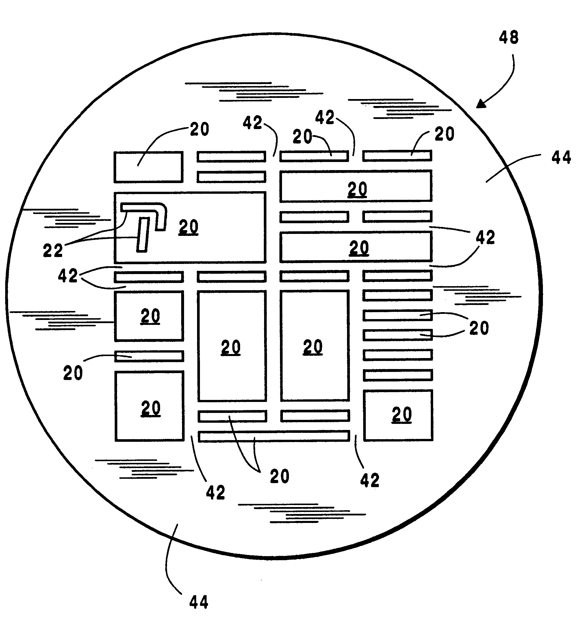
In describing the preferred embodiment of the present invention, reference will be made herein to FIGS. 4-6 of the drawings in which like numerals refer to like features of the invention. Features of the invention are not necessarily shown to scale in the drawings.

Typical materials used in the past for membrane layers include doped-silicon and silicon-nitride (SiN). Such materials have a Young's modulus in the 160 GPa range. Instead of such conventional materials, the present invention uses other materials as PEBL mask membranes. Advanced materials, such as silicon carbide (SiC), diamond, and diamond-like carbon (DLC) have been found to have a more robust structure, which has been linked to their much higher Young's modulus of elasticity. The Young's modulus of diamond is approximately 1000 GPa, and the Young's modulus for SiC is about 480 GPa. The Young's modulus of DLC can vary depending on manufacturing, but can be made by conventional techniques with higher values. This means t...


PUM

PropertyMeasurementUnit
Young's modulusaaaaaaaaaa
thicknessaaaaaaaaaa
thicknessaaaaaaaaaa

Abstract

A stencil or scatterer mask for use with charged particle beam lithography such as projection electron-beam lithography comprises a membrane layer of a material having a Young's modulus of at least about 400 GPa and support struts supporting a surface of the membrane. The struts form and surrounding a plurality of discrete membrane areas of different aspect ratios aligned to design regions of an integrated circuit. The discrete membrane areas have different aspect ratios range from about 1:1 to about 12:1, and the discrete membrane areas have different size surface areas. The membrane is preferably silicon carbide, diamond, diamond-like carbon, amorphous carbon, carbon nitride or boron nitride. When used in scatterer masks, the ratio of discrete membrane area to membrane thickness is at least about 0.18 mm2/nm. When used in stencil masks, the ratio of discrete membrane area to membrane thickness is at least about 1.0 mm2/nm. The stencil mask is made by depositing a diamond membrane film patterned with a hardmask layer on a substrate, depositing an etch stop layer adjacent the diamond film, and forming supporting struts surrounding a plurality of discrete areas of the membrane film. The method then includes depositing a pattern over the membrane film within the discrete membrane film areas, the pattern conforming to one or more desired circuit elements, and etching the membrane film with a reactive ion etch containing oxygen to form openings in the membrane film.

Description

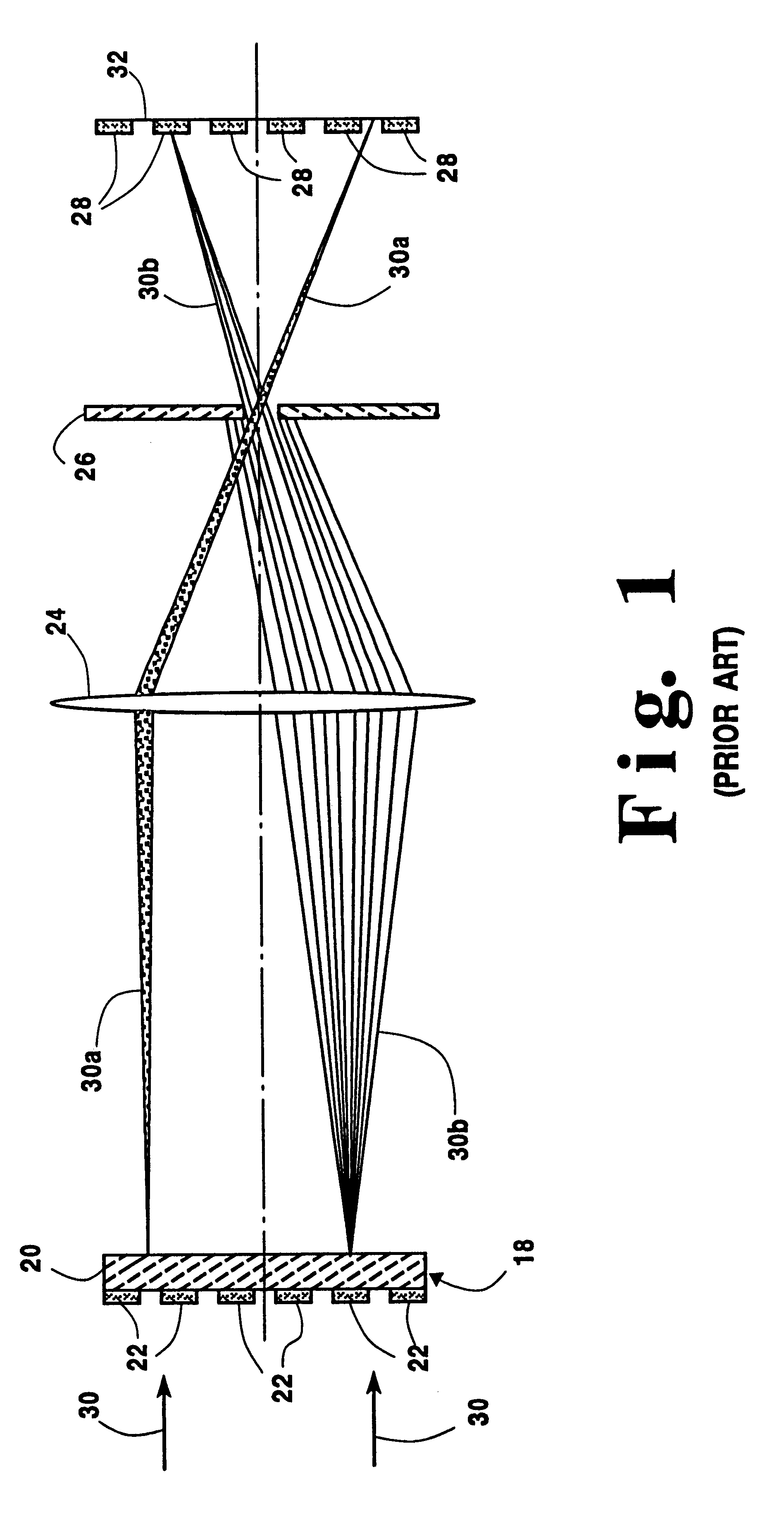
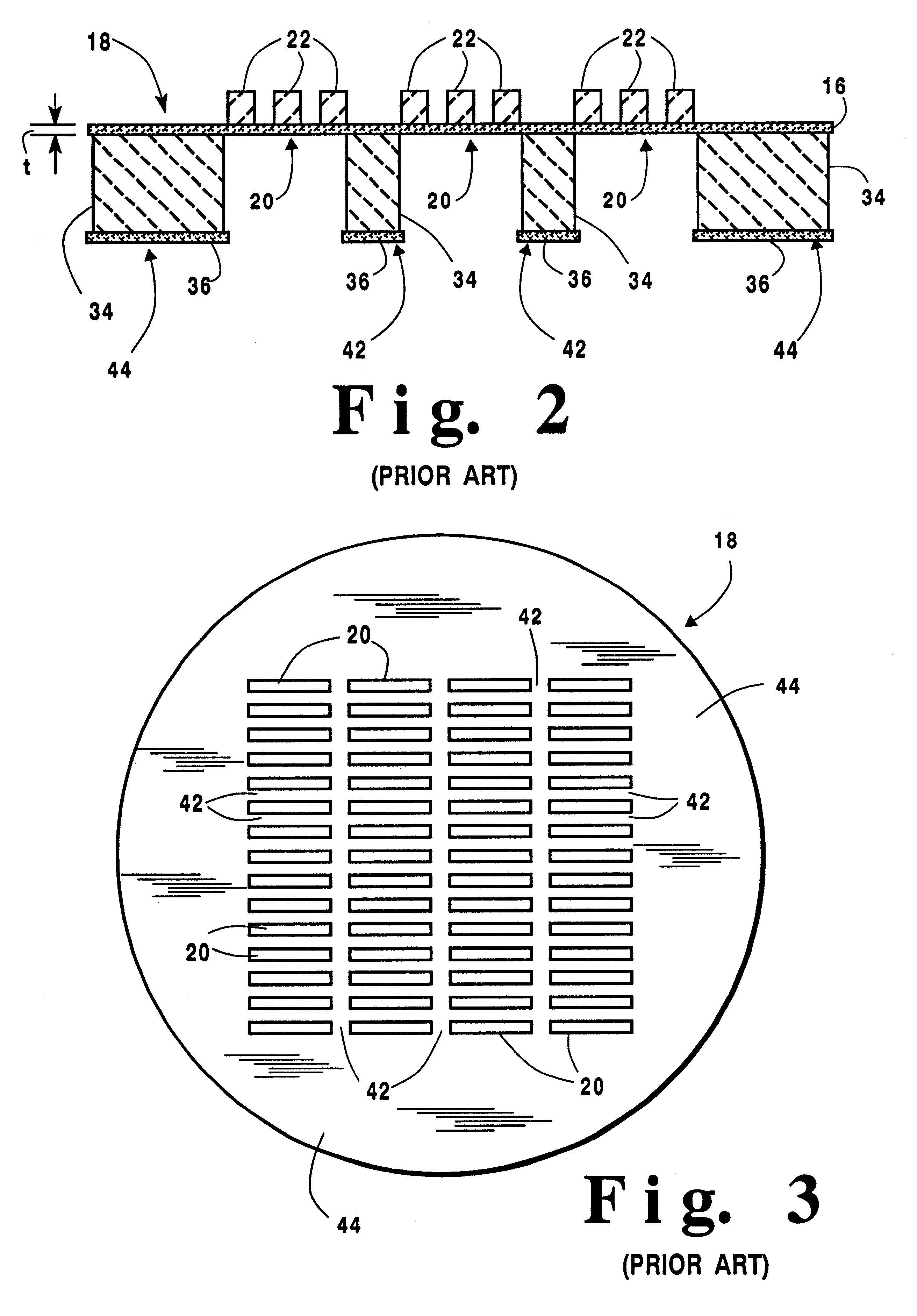
1. Field of the InventionThe present invention relates to masks used in photolithography of integrated circuit designs, and in particular, masks used in ray or charged particle beam lithography.2. Description of Related ArtOne of the most critical parameters of masks fabricated for advanced photolithography of integrated circuit designs is image placement error. This is particularly important for membrane masks such as those used in x-ray or charged particle beam lithography such as ion beam and, in particular, projection electron-beam lithography (PEBL). An embodiment of PEBL is referred to as the SCALPEL.TM. (scattering angular limited projection electron lithography) process. Projection electron-beam lithography requires masks that are at least semi-transparent to electrons. For this reason, these masks contain membranes that are very thin, on the order of 50-200 nm.An example of the well-known PEBL lithography is shown in FIG. 1. Electron beam radiation 30 passes through a porti...

Claims


Application Information

Patent Timeline
Patent Type & Authority Patents(United States)
IPC IPC(8): G03F1/14G03F1/16G03F1/20H01L21/027
CPCG03F1/20H01J2237/31794H01J2237/0453G03F1/50G03F1/54G03F1/64
Inventor BROOKS, CAMERON J.LERCEL, MICHAEL J.POWERS, LYNN A.
Owner IBM CORP
Why Eureka
Try Eureka