
Thinner composition and methods and systems for using the thinner composition

a composition and thin technology, applied in the field of thin compositions, can solve the problems of reducing productivity, affecting the production efficiency of electronic devices, and affecting the quality of thin compositions,

Inactive Publication Date: 2001-07-17
SAMSUNG ELECTRONICS CO LTD
View PDF6 Cites 8 Cited by
  • Summary
  • Abstract
  • Description
  • Claims
  • Application Information

AI Technical Summary

Problems solved by technology

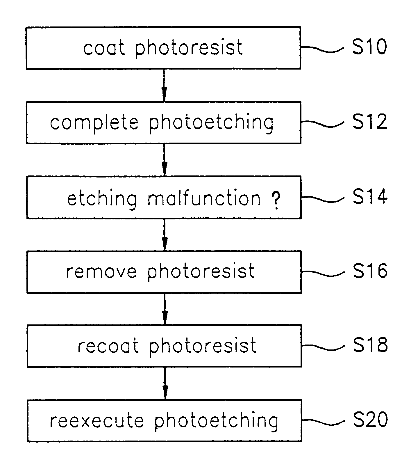
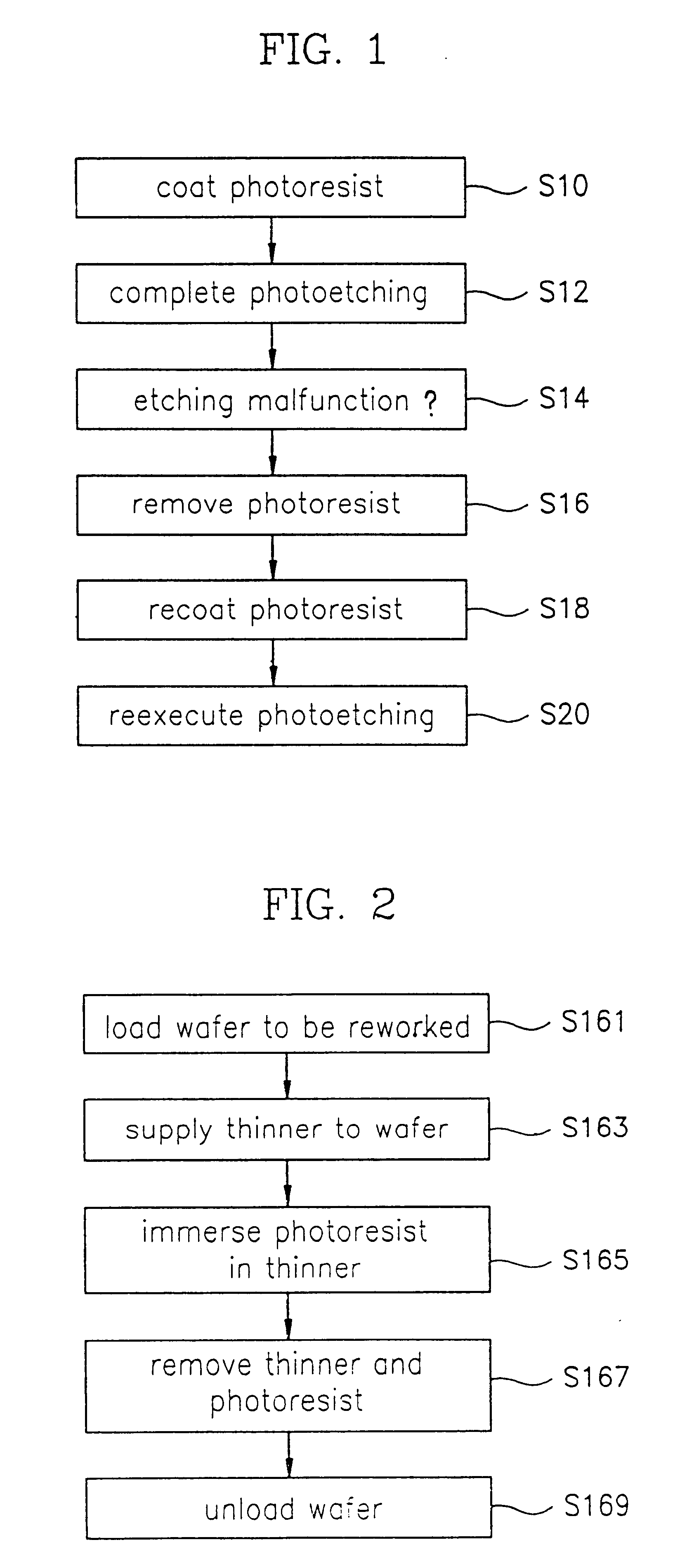
Occasionally, the photoetching process results in failure.
Additionally, complications can occur if the photoresist applied in the second photoetching process is incompatible with the thinner used when reworking the substrate.
Conventionally, this incompatibility dictated that a different thinner or rework apparatus had to be used.
Having multiple rework apparatuses decreases productivity and increases cost.
A second problem associated with conventional thinners is that many of the conventional thinners with the necessary solubility, volatility, and viscosity for use in reworking a substrate or for use in a rinse process are toxic.
Ethyleneglycol monoethylether acetate (ECA) has a good solubility rate, however, its volatility and flammability is unacceptably high, further, it is toxic to humans if inhaled or contacted on the skin.
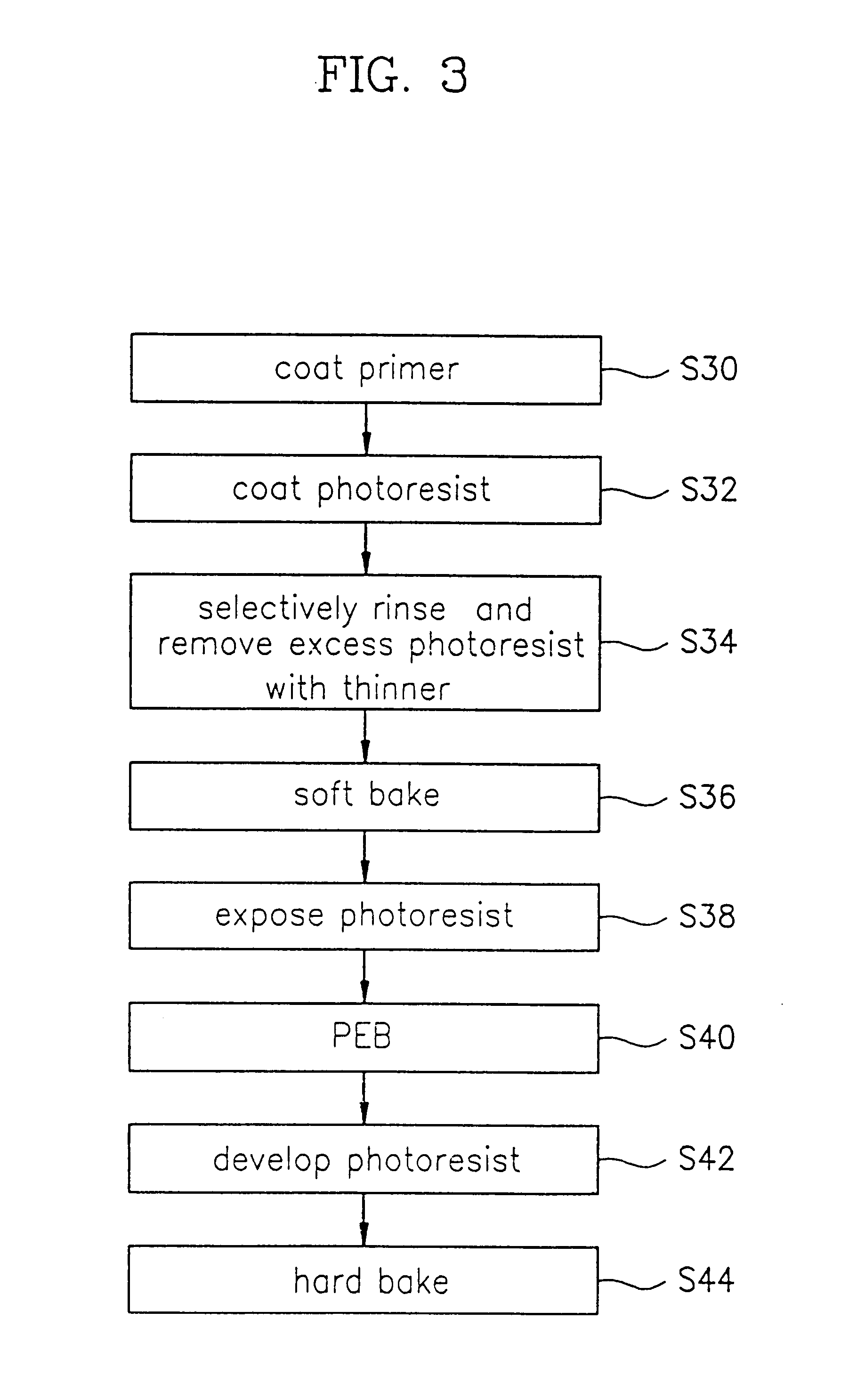
Unwanted photoresist remaining on the edges or the backside of the wafer can cause etching failure or can generate particle contamination during subsequent processing, such as during etching or ion-injection, thereby decreasing the production yield.
This reduces the yield of the semiconductor devices.
If the viscosity is too high, an excessively high spraying pressure is required.
If viscosity is too low, the spray focus will deteriorate because the thinner cannot be concentrated or focused on the contact position of the wafer which interferes with the ability of the thinner to selectively remove unwanted photoresist during rinsing.
Methyl isobutyl ketone (MIBK) is now widely used for rinsing photoresist, however, its high volatility can give operators headaches.
Further, it can contaminate the air inside a cleanroom, cause accumulation of photoresist on the edge of the wafer because of its high volatility rate on the surface of the wafer, and cause photoresist powder to stick to the exhaust duct, thereby requiring frequent cleaning of the exhaust duct.
However, this solvent cannot be sprayed onto a wafer to selectively remove the unwanted photoresist (i.e., remove the photoresist from the edge and backside portions of the wafer) because the viscosity is too high.
Specifically, the '280 patent discloses mixing of 1,2-ethoxyl acetate, methyl ethyl ketone (MEK), xylene, and n-butyl acetate (n-BA), or use of mixtures including two or more of these chemicals, but the '280 patent does not disclose using the mixture for rinsing.

Method used


Image

  • Thinner composition and methods and systems for using the thinner composition
  • Thinner composition and methods and systems for using the thinner composition
  • Thinner composition and methods and systems for using the thinner composition

Examples


Embodiment Construction

The conventional thinner methyl isobutyl ketone (MIBK) was compared to the thinners contemplated by the present invention. The solubility rate and the volatility of each were measured in the same manner as in the "Embodiments 1 to 12" section. The results are shown in Table 1. Note that while the specific volatility rates for Comp. Ex. 2 and Comp. Ex. 3 are not identified in Table 1, the volatility rates for EA and MMP are higher than nBA, the ratio generally being on the order of nBA:EA:MMP=1:5:3.

As shown in the Table 1, and as compared with the conventional methyl isobutyl ketone (MIBK), the thinner composition comprising a mixture of n-butyl acetate (n-BA) and ethyl acetate (EA) by mixing ratio of (8 to 9):(2 to 1), or a mixture of n-butyl acetate (n-BA) and methyl methoxy propionate (MMP) by mixing ratio of (7 to 8):(3 to 2), or a mixture of n-butyl acetate (n-BA) and methyl ethyl ketone (MEK) by mixing ratio of (8 to 9):(2 to 1) shows a solubility rate similar to that of the me...


PUM

PropertyMeasurementUnit
temperatureaaaaaaaaaa
thicknessaaaaaaaaaa
diameteraaaaaaaaaa

Abstract

Thinner compositions for effectively removing photoresist. The thinner compositions may be used in reworking a semiconductor substrate or in rinsing semiconductor devices. The thinner composition may be a mixture of n-butyl acetate (n-BA) and ethyl acetate (EA), a mixture of n-butyl acetate (n-BA) and methyl methoxy propionate (MMP), or a mixture of n-butyl acetate (n-BA) and methyl ethyl ketone (MEK).

Description

1. Field of the InventionThe present invention relates to the field of electronic device fabrication including semiconductor device fabrication, and flat panel display fabrication, preferably Liquid Crystal Display (LCD) fabrication, and more particularly, to thinner compositions for selectively removing photoresist.2. Description of the Related ArtPhotoetching is used to form circuit patterns on semiconductor substrates or flat panel display substrates, for example, glass or quartz, on specific layers that have previously been formed on the substrate. Photoetching is typically carried out by coating photoresist on the substrate and causing a photo-chemical reaction on the substrate.More particularly, a photoetching process typically involves first coating a primer over the semiconductor substrate. The primer improves the adhesiveness of the photoresist to the substrate. The photoresist is then coated onto the primer. A rinsing step is used to remove unwanted photoresist that was co...

Claims


Application Information

Patent Timeline
Patent Type & Authority Patents(United States)
IPC IPC(8): G03F7/42H01L21/02H01L21/311H01L21/306
CPCH01L21/31133G03F7/422H01L21/306
Inventor JEON, MI-SOOK
Owner SAMSUNG ELECTRONICS CO LTD
Learn More