CVD plasma assisted low dielectric constant films

a dielectric constant and plasma technology, applied in the field of integrated circuit fabrication, can solve the problems of damage to the device structure, inadequate etch stop layer material, and degrade the overall performance of the devi

Inactive Publication Date: 2001-09-11
APPLIED MATERIALS INC
View PDF123 Cites 239 Cited by
  • Summary
  • Abstract
  • Description
  • Claims
  • Application Information

AI Technical Summary

Problems solved by technology

The high temperatures at which some thermal CVD processes operate can damage device structures having layers previously formed on the substrate.
However, the barrier/liner layers typically have dielectric constants that are significantly greater than 4.0, and the high dielectric constants result in a combined insulator that does not significantly reduce the dielectric constant.
Furthermore, known low k dielectric materi...

Method used


Image

  • CVD plasma assisted low dielectric constant films
  • CVD plasma assisted low dielectric constant films
  • CVD plasma assisted low dielectric constant films

Examples


examples

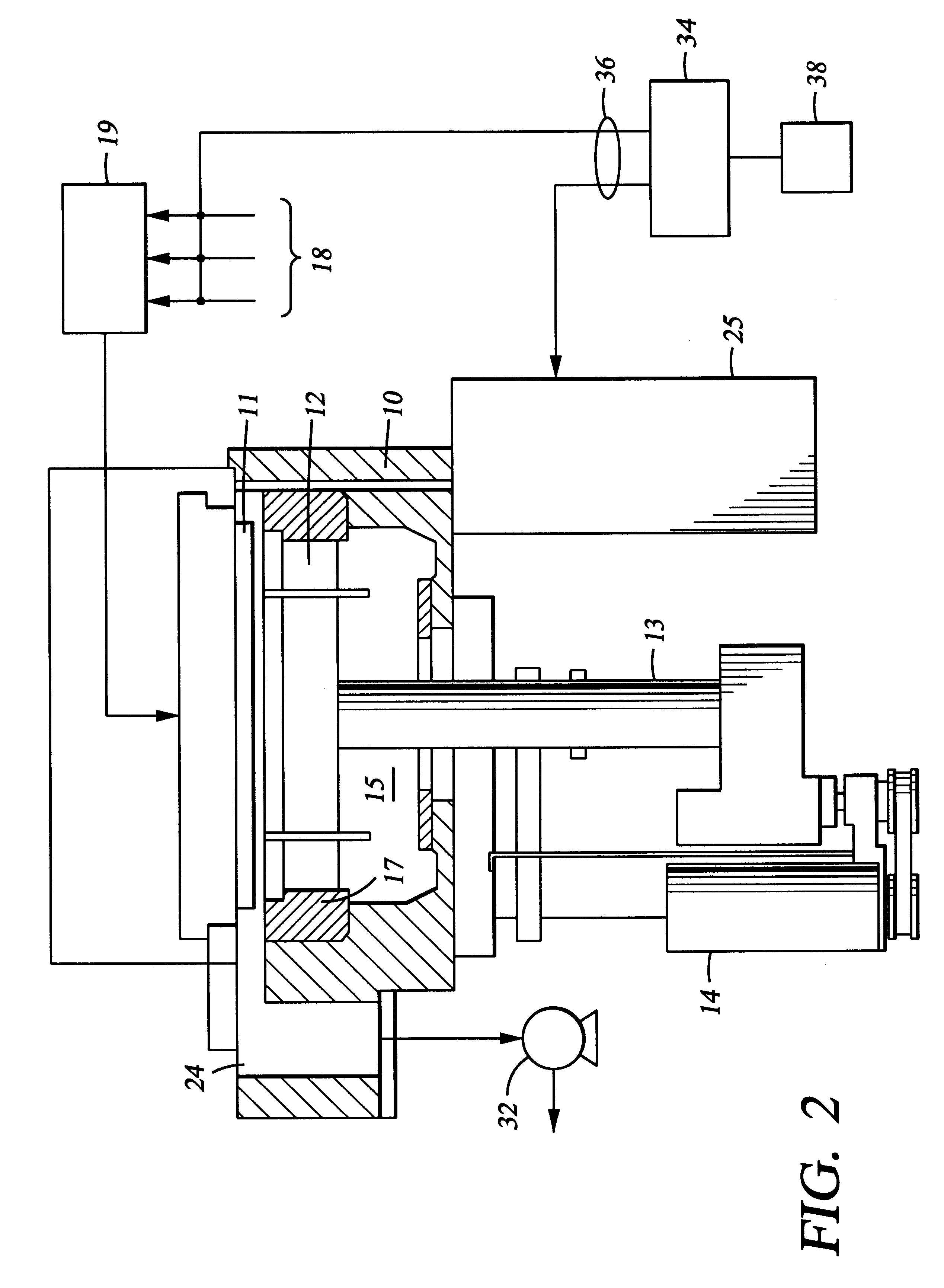
The following examples demonstrate deposition of an oxidized organosilane or organosiloxane film having excellent barrier and adhesion properties. This example was undertaken using a chemical vapor deposition chamber, and in particular, a "CENTURA DxZ" system which includes a solid-state RF matching unit with a two-piece quartz process kit, both fabricated and sold by Applied Materials, Inc., Santa Clara, Calif.

Non-Pulsed RF Power

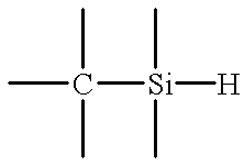
An oxidized dimethylsilane film was deposited at a chamber pressure of 3.0 Torr and temperature of 15.degree. C. from reactive gases which were flowed into the reactor as follows:

The substrate was positioned 600 mil from the gas distribution showerhead and 20 W of high frequency power (13 MHz) was applied to the showerhead for plasma enhanced deposition of an oxidized dimethylsilane layer. The oxidized dimethylsilane material had a dielectric constant of about 2.5 and was hydrophobic.

Pulsed RF Power (Hypothetical)

An oxidized 1,3,5-trisilano-2,4,6-trimethyle...


PUM

PropertyMeasurementUnit
Fractionaaaaaaaaaa
Fractionaaaaaaaaaa
Angleaaaaaaaaaa

Abstract

A method and apparatus for depositing a low dielectric constant film by reaction of an organosilane or organosiloxane compound and an oxidizing gas at a low RF power level from 10-250 W. The oxidized organosilane or organosiloxane film has good barrier properties for use as a liner or cap layer adjacent other dielectric layers. The oxidized organosilane or organosiloxane film may also be used as an etch stop or an intermetal dielectric layer for fabricating dual damascene structures. The oxidized organosilane or organosiloxane films also provide excellent adhesion between different dielectric layers. A preferred oxidized organosilane film is produced by reaction of methylsilane, CH3SiH3, or dimethylsilane, (CH3)2SiH2, and nitrous oxide, N2O, at an RF power level from about 10 to 200 W or a pulsed RF power level from about 20 to 250 W during 10-30% of the duty cycle.

Description

BACKGROUND OF THE DISCLOSURE1. Field of the InventionThe present invention relates to the fabrication of integrated circuits. More particularly, the invention relates to a process and apparatus for depositing dielectric layers on a substrate.2. Background of the InventionOne of the primary steps in the fabrication of modern semiconductor devices is the formation of metal and dielectric films on a substrate by chemical reaction of gases. Such deposition processes are referred to as chemical vapor deposition or CVD. Conventional thermal CVD processes supply reactive gases to the substrate surface where heat-induced chemical reactions take place to produce a desired film. The high temperatures at which some thermal CVD processes operate can damage device structures having layers previously formed on the substrate. A preferred method of depositing metal and dielectric films at relatively low temperatures is plasma-enhanced CVD (PECVD) techniques such as described in U.S. Pat. No. 5,362,...

Claims


Application Information

Patent Timeline
IPC IPC(8): C23C16/40H01L21/768H01L21/02H01L21/70H01L21/316A01C15/02A01C17/00
CPCC23C16/401H01L21/02208H01L21/02274H01L21/0228H01L21/02304H01L21/02362H01L21/31612H01L21/76801H01L21/76808H01L21/7681H01L21/76829H01L21/76832H01L21/76834H01L21/76835H01L21/02126H01L2221/1031
Inventor CHEUNG, DAVIDYAU, WAI-FANMANDAL, ROBERT R.
Owner APPLIED MATERIALS INC
Why Eureka
Try Eureka