Organic electroluminescent device

an electroluminescent device and organic technology, applied in the direction of discharge tube luminescnet screens, other domestic articles, natural mineral layered products, etc., can solve the problems of easy oxidizability, unstable, and sensitive materials of organic layers formed, and achieve high efficiency, low cost, and high stability.

Inactive Publication Date: 2001-10-02
FUTABA CORPORATION
View PDF14 Cites 6 Cited by
  • Summary
  • Abstract
  • Description
  • Claims
  • Application Information

AI Technical Summary

Benefits of technology

According to the invention, organic EL devices having performance comparable to or more than prior art devices having a hole injecting and transporting layer or an electron injecting and transporting layer using organic materia...

Problems solved by technology

Reliability is a common problem to be solved for these organic EL devices.
However, the materials of which the organic layers are formed are vulnerable during manufacture and have less affinity to the electrodes.
These materials, however, are readily oxidizable and unstable, becoming the serious factor that governs the life of organic EL devices and gives rise to ...

Method used


Image

  • Organic electroluminescent device
  • Organic electroluminescent device
  • Organic electroluminescent device

Examples


example 1

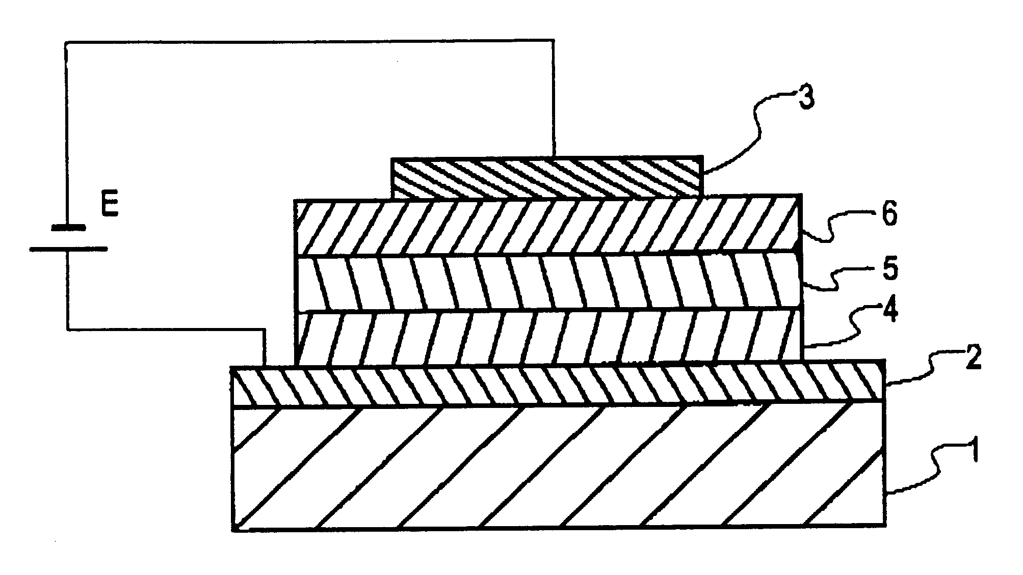
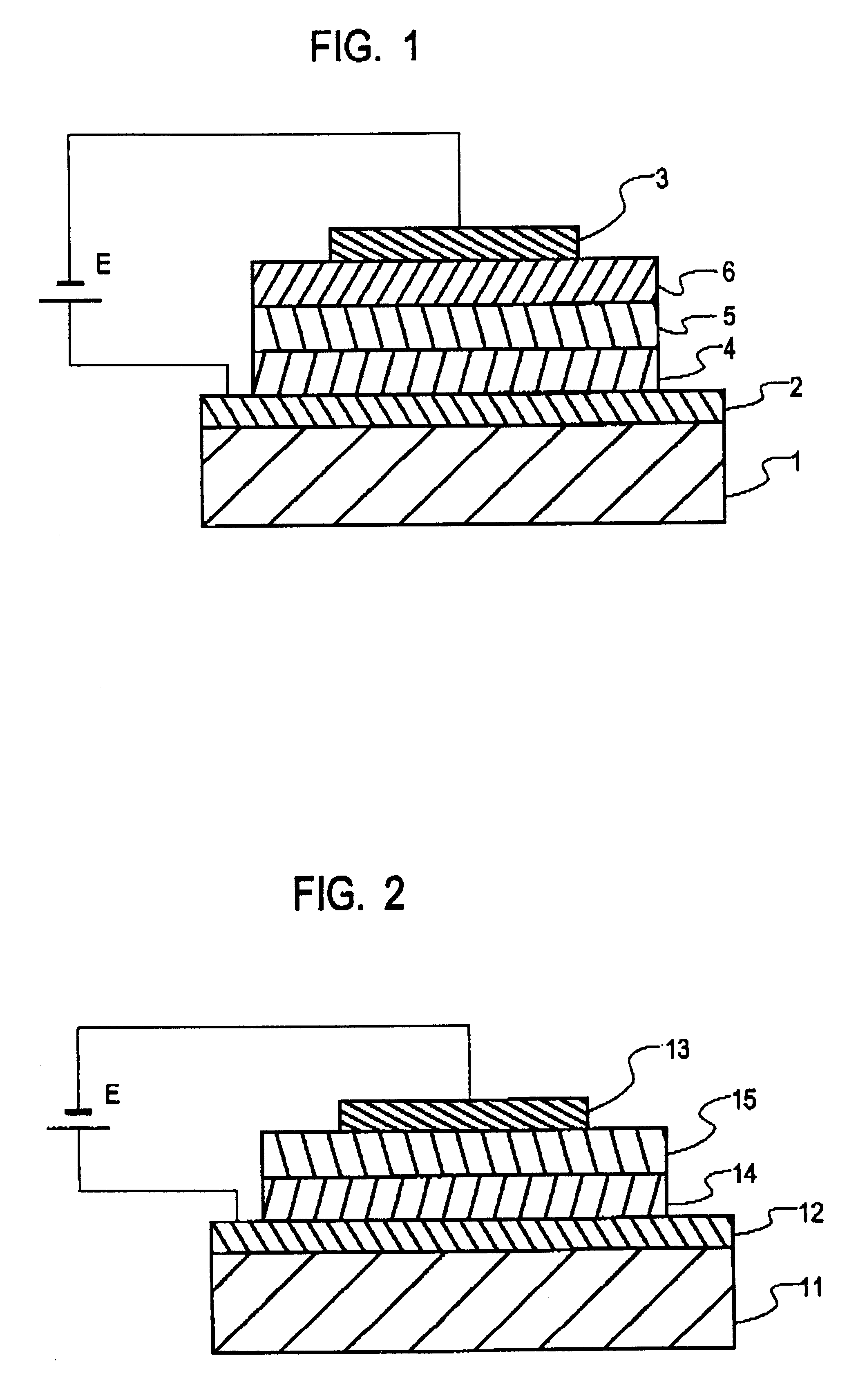
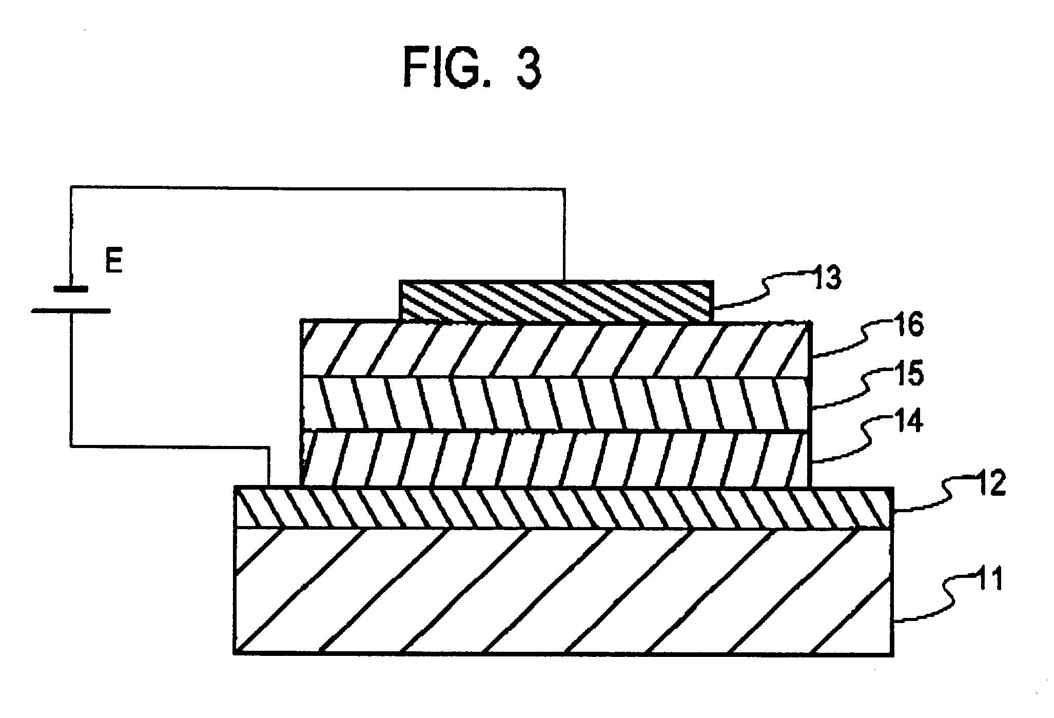
A substrate of (7059) glass by Corning Glass Works was scrubbed using a neutral detergent. The substrate was then secured by a holder in a sputtering apparatus where a hole injecting electrode layer of ITO was formed by a DC magnetron sputtering process using a target of ITO oxide.

The substrate having ITO deposited thereon was subjected to ultrasonic washing with neutral detergent, acetone, and ethanol, pulled up from boiling ethanol, and dried. After the surface was further cleaned with UV / O.sub.3, the substrate was secured by a holder in a spattering chamber, which was evacuated to a vacuum of 1.times.10.sup.-4 Pa or lower.

Next, using a target of SiO.sub.2, an inorganic insulative hole injecting layer was deposited to a thickness of 2 nm. The sputtering gas used was argon mixed with 5% of O.sub.2. Sputtering conditions included a substrate temperature of 25.degree. C., a deposition rate of 1 nm / min, an operating pressure of 0.5 Pa, and an input power of 5 W / cm.sup.2. The hole inje...

example 2

In Example 1, the main component and stabilizer of the inorganic electron injecting and transporting layer were changed from SrO to MgO, CaO or a mixture of these oxides, from Li.sub.2 O to K.sub.2 O, Rb.sub.2 O, K.sub.2 O, Na.sub.2 O, Cs.sub.2 O or a mixture of these oxides, and from SiO.sub.2 to GeO.sub.2 or a mixture of SiO.sub.2 and GeO.sub.2. Substantially equivalent results were obtained. Similar results were obtained when the negative electrode material was changed from Al to Ag, In, Ti, Cu, Au, Mo, W, Pt, Pd, Ni or an alloy thereof.

example 3

An organic EL device was fabricated as in Example 1 except that in the step of depositing the inorganic insulative hole injecting layer in Example 1, the composition of the target was changed to SiO.sub.2 and the flow rate of O.sub.2 in the sputtering gas was changed to a mixing ratio of 5% relative to Ar so that the layer had a composition of SiO.sub.1.9. On the lifetime test, substantially equivalent results were obtained.

Further, organic EL devices were similarly fabricated except that the composition of the target was changed to SiO.sub.2 and the flow rate of O.sub.2 in the sputtering gas was changed to a mixing ratio of 30% relative to Ar so that the layer had a composition of SiO.sub.1.95 ; the composition of the target was changed to GeO.sub.2 and the flow rate of O.sub.2 in the sputtering gas was changed to a mixing ratio of 30% relative to Ar so that the layer had a composition of GeO.sub.1.96 ; and the composition of the target was changed to SiO.sub.0.5 Ge.sub.0.5 O.sub.2...


PUM

PropertyMeasurementUnit
Thicknessaaaaaaaaaa
Thicknessaaaaaaaaaa
Electrical resistanceaaaaaaaaaa

Abstract

The invention provides an organic EL device comprising a substrate, a hole injecting electrode and a negative electrode formed on the substrate, a light emitting layer containing an organic material between the electrodes, an inorganic electron injecting and transporting layer between the light emitting layer and the negative electrode, and an inorganic insulative hole injecting and transporting layer between the light emitting layer and the hole injecting electrode. The inorganic electron injecting and transporting layer contains at least one oxide selected from among strontium oxide, magnesium oxide, calcium oxide, lithium oxide, rubidium oxide, potassium oxide, sodium oxide, and cesium oxide as a main component and silicon oxide and/or germanium oxide as a stabilizer. The inorganic insulative hole injecting and transporting layer (4) contains silicon oxide and/or germanium oxide as a main component, the main component having an average composition represented by the formula:wherein 0<=x<=1 and 1.7<=y<=1.99, as analyzed by Rutherford back-scattering. Organic EL devices having performance comparable to or more than that of prior art devices having a hole injecting and transporting layer or an electron injecting and transporting layer using organic materials, a long life, weather resistance, high stability, high efficiency, and low cost are realized. The devices are easy to manufacture and have stable physical properties at the film interface even when the light emitting layer consists of two or more layers.

Description

1. Technical FieldThis invention relates to an organic electroluminescent (EL) device and more particularly, to an inorganic / organic junction structure suitable for use in a device of the type wherein an electric field is applied to a thin film of an organic compound to emit light.2. Background ArtIn general, organic EL devices have a basic configuration including a glass substrate, a transparent electrode of ITO etc., a hole transporting layer of an organic amine compound, an organic light emitting layer of a material exhibiting electronic conductivity and intense light emission such as Alq3, and an electrode of a low work function metal such as MgAg, wherein the layers are stacked on the substrate in the described order.The device configurations which have been reported thus far have one or more organic compound layers interposed between a hole injecting electrode and an electron injecting electrode. The organic compound layers are typically of two- or three-layer structure.Includ...

Claims


Application Information

Patent Timeline
IPC IPC(8): H01L51/50H01L51/52H05B33/12H05B33/14H05B33/22
CPCH01L51/5088H01L51/5092Y10S428/917H10K50/171H10K50/17
Inventor ARAI, MICHIOKOBORI, ISAMUMITSUHASHI, ETSUO
Owner FUTABA CORPORATION
Why Eureka
Try Eureka