Processing low dielectric constant materials for high speed electronics

a technology of low dielectric constant and high-speed electronics, applied in the direction of dielectric characteristics, dielectric resistance improvement, high-frequency circuit adaptation, etc., can solve the problems of high loading, semiconductor chips cannot drive low reactive impedance, and inherent limitations of high-frequency applications of electronic circuits

Inactive Publication Date: 2001-10-02
SABIC INNOVATIVE PLASTICS IP BV
View PDF19 Cites 34 Cited by
  • Summary
  • Abstract
  • Description
  • Claims
  • Application Information

AI Technical Summary

Benefits of technology

Another object of this invention is to provide a method for processing low dielectric constant porous materials which does not leave process chemicals behind in the porous materials.
Porous PTFE material is approximately 70% air and is generally made by stretching PTFE to cause approximately nine billion holes per square inch to be distributed evenly throughout its volume. The resulting structure is a filter type material in that gas or liquid can pass through the interconnected pores. This porous structure is composed of mostly air and can readily be filled with a sublimable material. The resulting porous material can be used as a low dielectric constant material in the manufacture of high frequency circuits and can reduce the need for laser ablation of material situated over air bridge structures and other microwave structures and devices.

Problems solved by technology

Electronic circuits have inherent limitations in high frequency applications.
In high frequency circuits capacitive loading becomes so high that a semiconductor chip cannot drive the low reactive impedance.
Because these high frequency circuits have historically been power inefficient, their usefulness in airborne and satellite applications is limited.
(GORE-TEX is a trademark of W.L. Gore & Associates, Inc., of Newark, Del.) have excellent low dielectric constant properties, but unfortunately they absorb process chemicals in their pores during MCM (multi-chip module) or PC (printed circuit) board processing that cannot be removed.
Additionally, the fact that the porous material becomes crushed during pressurized processing destroys its porous properties, and therefore the deformed material does not provide the desired consistent low dielectric constant.
These sensitive air bridge structures create processing challenges for both the manufacturer and the end user.
Filling the pores with a material such as an acrylate glue enables use of the material as a laminant film; however, this causes the resultant dielectric constant to degrade and limits the material's usefulness at high frequencies.
However, in laminant applications and processing, the pores can collapse under pressure and / or be filled with processing materials during fabrication which cannot be easily removed.
These materials, however, are inflexible and not fabricated in large area sections.
Because the ceramic foam materials are inflexible and cannot be stretched, they can be used as substrates but cannot be used in overlay technologies that are not perfectly flat.
Because ceramic foam materials are fragile, they are typically not capable of withstanding PC board lamination processing in their intrinsic state.
Another problem common to both porous PTFE material and ceramic foam material is that if the porous / foam material is to be used in any process in which a metallization layer is applied over the material, the metal tends to extend into the pores and it is thus difficult to achieve a smooth and continuous metal surface for use in high frequency applications where skin-effect related losses are of importance.
Few intrinsically low dielectric constant materials can withstand the high temperatures in commercial and military processing.
Most of the low dielectric constant materials that can withstand higher temperatures are only absorptive below the 200 nanometer wavelength region of the light spectrum, and thus it is nearly impossible to process those materials using ion argon and other CW (continuous wave) lasers.

Method used


Image

  • Processing low dielectric constant materials for high speed electronics
  • Processing low dielectric constant materials for high speed electronics
  • Processing low dielectric constant materials for high speed electronics

Examples


Embodiment Construction

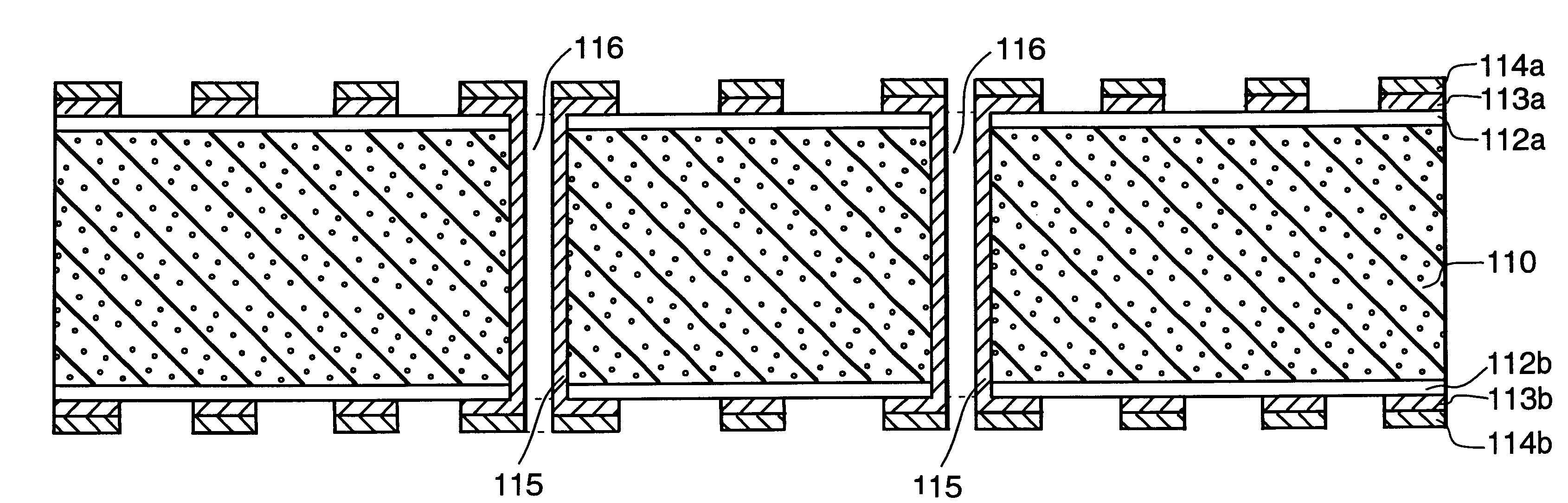
FIG. 1 is a sectional side view of a porous layer 110 filled with additive material. In one embodiment porous layer 110 comprises a porous PTFE material. In one example, the pores have diameters ranging approximately from 0.01 to 5 .mu.m. Expanded PTFE is a useful porous layer because it does not dissolve in most of the fabricating chemicals and because it is sponge-like (permeable) so that additive material can be readily dispersed evenly throughout the layer. Other examples of potentially useful porous material include polyethylene and polystyrene, for example. Thicknesses of the porous material typically range from several microns to tens of mils so that mechanical stability of the PC boards can be maintained. Preferably the porous material is flexible enough so that it can be shaped to accommodate non-planar surfaces but is rigid enough that it does not sag.

The selected additive material must be capable of withstanding high processing temperatures and pressures and capable of re...


PUM

PropertyMeasurementUnit
dielectric constantaaaaaaaaaa
dielectric constantsaaaaaaaaaa

Abstract

A low dielectric constant printed circuit board includes: a low dielectric constant porous polymer layer having holes therethrough, the porous layer having pores; and a patterned metallization layer over surfaces of the low dielectric constant porous polymer layer and surfaces of the holes, the patterned metallization layer not significantly protruding into the pores of the porous layer.

Description

1. Field of the InventionThis invention relates generally to low dielectric constant porous materials and, more particularly, to a process for using porous layers in printed circuit boards.2. Description of the Related ArtElectronic circuits have inherent limitations in high frequency applications. For example, capacitive loading is increased at higher frequencies because capacitive reactance is directly proportional to frequency. In high frequency circuits capacitive loading becomes so high that a semiconductor chip cannot drive the low reactive impedance. Because these high frequency circuits have historically been power inefficient, their usefulness in airborne and satellite applications is limited.Porous polytetrafluoroethylene (PTFE) materials such as GORE-TEXT.RTM. (GORE-TEX is a trademark of W.L. Gore & Associates, Inc., of Newark, Del.) have excellent low dielectric constant properties, but unfortunately they absorb process chemicals in their pores during MCM (multi-chip mod...

Claims


Application Information

Patent Timeline
Patent Type & Authority Patents(United States)
IPC IPC(8): H05K1/09H05K1/02H05K3/38
CPCH05K1/024H05K3/386H05K2201/0116H05K2201/015Y10T29/49155Y10T428/24917Y10T29/49165Y10T29/49124H05K2201/0158
Inventor WOJNAROWSKI, ROBERT JOHNCOLE, HERBERT STANLEYSITNIK-NIETERS, THERESA ANNDAUM, WOLFGANG
Owner SABIC INNOVATIVE PLASTICS IP BV
Why Eureka
Try Eureka