

Semiconductor light emitting element, and its manufacturing method
a technology of light-emitting elements and semiconductors, applied in the direction of basic electric elements, semiconductor devices, electrical equipment, etc., can solve the problems of large crystal defects in the crystal grown thereby, achieve easy and reliable separation, and overcome the deterioration of the crystalline property due to lattice mismatching with the sapphire substrate. , the effect of high quality
- Summary
- Abstract
- Description
- Claims
- Application Information
AI Technical Summary
Benefits of technology
Problems solved by technology
Method used
Image

Examples
first embodiment
First explained is a method for separating a substrate using a "lift-off layer" as the invention.
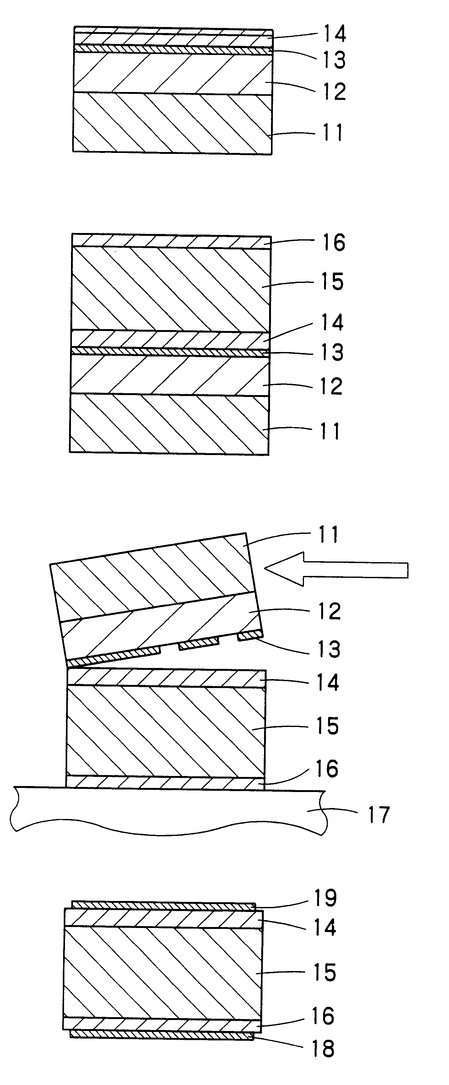
FIGS. 1A through 1D are cross-sectional views showing different steps of a manufacturing method of a semiconductor light emitting element according to the first embodiment. That is, these figures illustrate a manufacturing method of a semiconductor laser using nitride semiconductors.
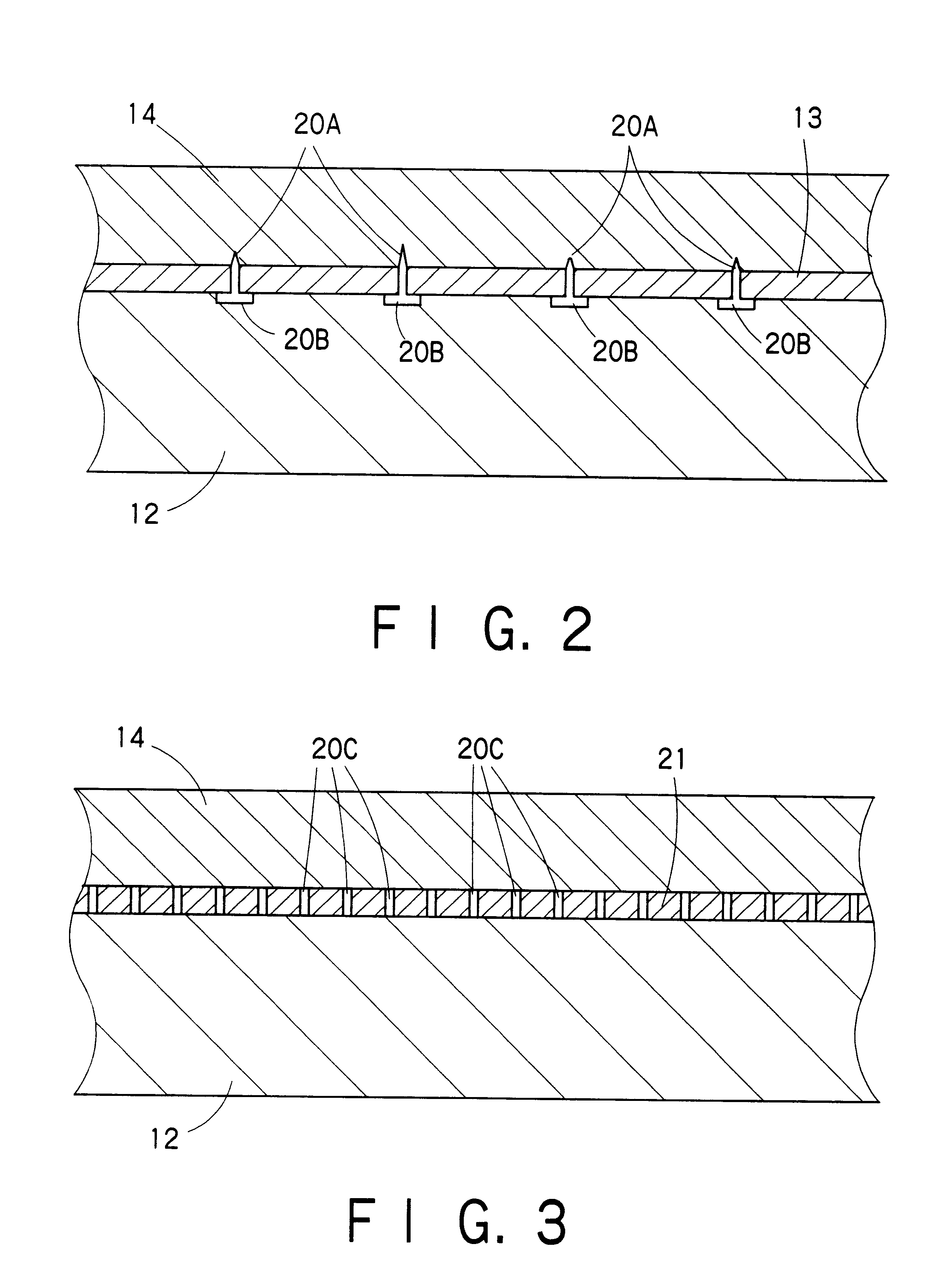
First referring to FIG. 1A, a GaN layer 12, AlGaN layer 13 and n-type GaN layer 14 are grown on a sapphire substrate 11 by MOCVD (metal organic chemical vapor deposition). A buffer layer, not shown, may be provided between the substrate 11 and the GaN layer 12. A normal pressure was used for growth of these layers. The layers other than the buffer layer, namely, GaN layers 12, 14 and AlGaN layer 13 were grown in an atmosphere basically mixing nitrogen, hydrogen and ammonium in a temperature range from 1000.degree. C. to 1100.degree. C.
The Al composition in the AlGaN layer 13 is approximately 30%, and it is fo...
second embodiment
Next explained is the invention configured to easily and reliably separate the substrate by previously processing the surface of the substrate of sapphire, for example, and thereafter epitaxially growing nitride semiconductor layers.
FIGS. 6A through 6D are schematic diagrams for explaining the second embodiment of the invention. That is, FIGS. 6A through 6D are cross-sectional views of the substrate portion under different steps of a manufacturing process. Numeral 101 refers to a sapphire substrate, 102 to voids, 103 to a GaN epitaxial layer, and 104 to poly-crystallized GaN.
In this embodiment, first referring to FIG. 6A, recesses are made on the surface of the sapphire substrate 101. More specifically, a mask, not shown, is applied onto the sapphire substrate 101, and grooves, 2 .mu.m wide and 3 .mu.m deep, are made on the sapphire substrate 101 by dry etching. These grooves function as the abruption mechanism susceptible to a stress.
After removing the mask, as shown in FIG. 6B, th...
third embodiment
Next explained is the invention.
FIGS. 11A through 11C are fragmentary cross-sectional views showing steps of the manufacturing process according to the third embodiment. FIG. 12 is a cross-sectional view schematically showing a laser device manufactured by the manufacturing method according to the embodiment.
First explained is the structure of the laser device shown in FIG. 12. Reference numeral 402 denotes a p-side electrode, 403 is a p-type GaN contact layer (Mg-doped by 3.about.5.times.10.sup.19 cm.sup.-3 and 0.1 .mu.m thick), 404 is a first AlGaN cladding layer (Mg-doped by 3.about.5.times.10.sup.18 cm.sup.-3 and 0.7 .mu.m thick), 405 is an AlGaN current blocking layer (Si-doped by 3.about.5.times.10.sup.18 cm.sup.-3 and 0.2 .mu.m thick), 406 is a second AlGaN cladding layer (Mg-doped by 3.about.5.times.10.sup.18 cm.sup.-3 and 0.1 .mu.m thick), 407 is an AlGaN overflow preventing layer, 408 is a GaN guide layer (undoped and 0.1 .mu.m thick), 409 is a MQW (three cycles of In.sub....
PUM
| Property | Measurement | Unit |
|---|---|---|
| oscillation wavelengths | aaaaa | aaaaa |
| oscillation wavelengths | aaaaa | aaaaa |
| oscillation wavelength | aaaaa | aaaaa |
Abstract
Description
Claims
Application Information