Register transfer level power optimization with emphasis on glitch analysis and reduction

a technology of register transfer and power optimization, applied in pulse manipulation, pulse technique, instruments, etc., can solve the problems of increasing chip packaging and cooling costs, increasing the total system cost, and few automated design and synthesis techniques for reducing glitching power consumption in general circuits

Inactive Publication Date: 2001-11-27
NEC CORP
View PDF7 Cites 59 Cited by
  • Summary
  • Abstract
  • Description
  • Claims
  • Application Information

AI Technical Summary

Problems solved by technology

Excessive power consumption also leads to an increase in chip packaging and cooling costs, which increase the total system cost.
However, very few automated design and synthesis techniques exist for reducing glitching power consumption in general circuits.
However, the power consumed by the functional units constitutes a small fraction of the...

Method used


Image

  • Register transfer level power optimization with emphasis on glitch analysis and reduction
  • Register transfer level power optimization with emphasis on glitch analysis and reduction
  • Register transfer level power optimization with emphasis on glitch analysis and reduction

Examples


example 2

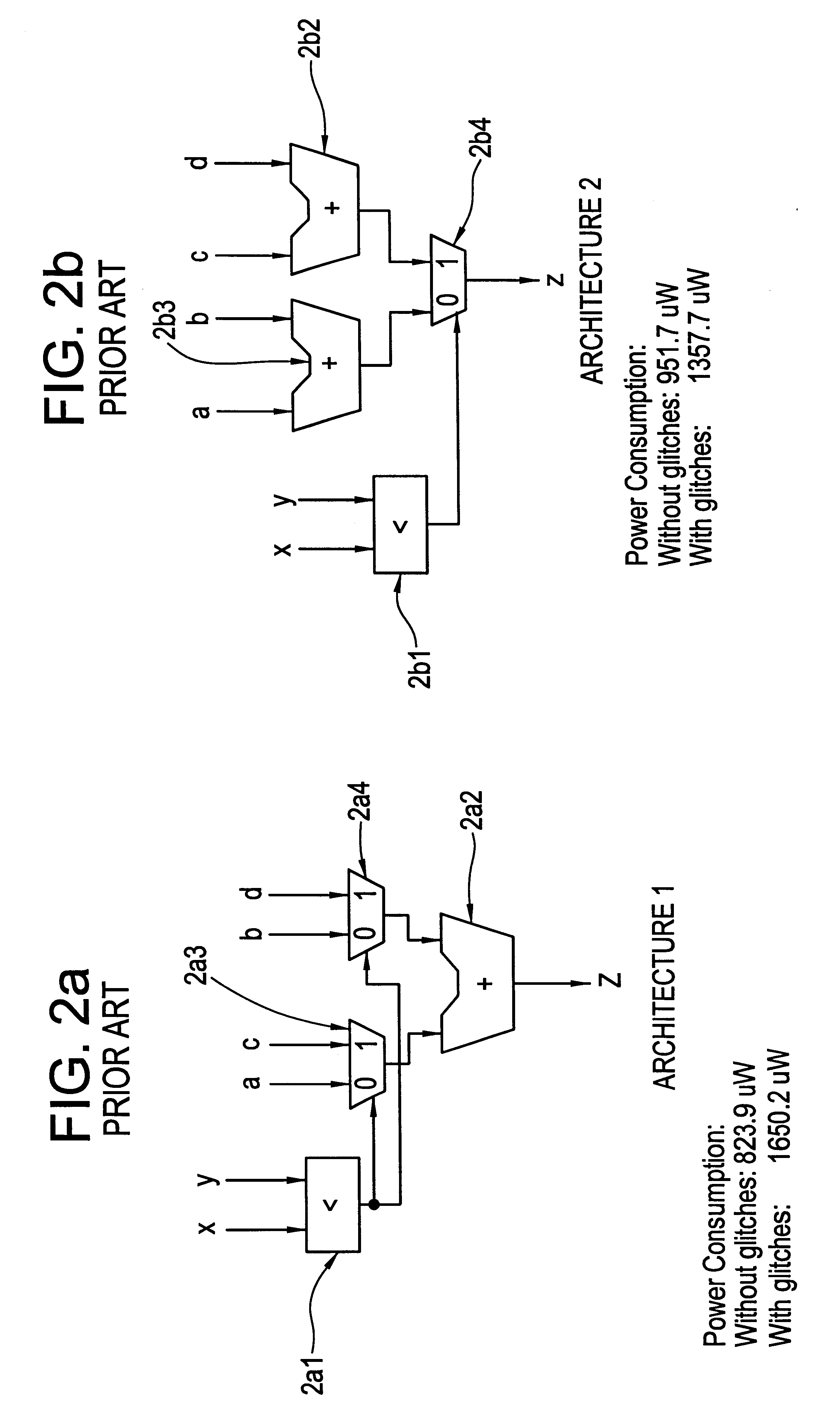
The elements shown in FIG. 3--a subtractor 31, an equal-to comparator 32, a less-than comparator 33 , and a 3-to-1 multiplexer tree 34 & 35--are representative data path blocks for studying glitch generation. The registers do not generate glitches at their outputs. To Study generation and propagation of glitches within above data path blocks, each block is mapped to a library like the NEC CMOS6 library, and then simulated under long input sequences that consist of random vectors. The total number of bit-transitions (including glitches) at the block outputs and the number of zero-delay transitions (i.e., the number of transitions not counting glitches) are measured. The block outputs in FIG. 3 are annotated with the results, where the numbers indicate transitions with and without glitches, respectively. The results clearly indicate significant generation of glitches in various data path blocks. In the equal-to comparator 32, no glitches are generated due to the fact that all its path...

example 3

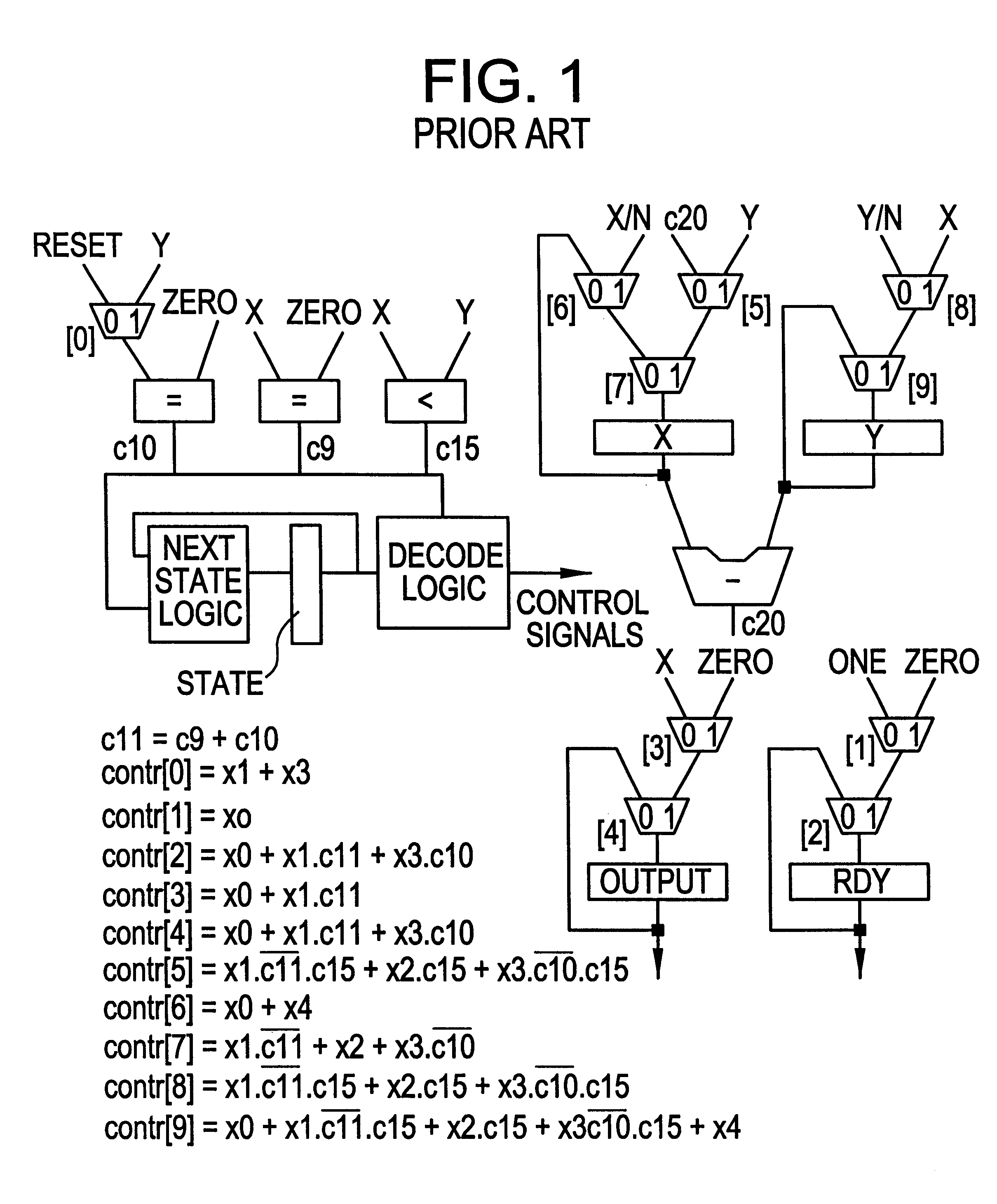
Control signal contr[2] in the RTL circuit shown in FIG. 1 is highly glitchy according to the statistics of Table 2. The portion of the decode logic that implements this control signal is shown in FIG. 4(a). It has been observed that though the inputs are largely glitch-free, significant glitches are generated at AND gates G1 and G2. Careful analysis shows that the generation of glitches is attributable to two conditions:

C1: A rising transition on signal x1 is frequently accompanied by a falling transition on c11. Thus, the rising transition on x1 and the falling transition on c11 are highly correlated.

C2: Transitions on signal x1 arrive earlier than transitions on signal c11.

Condition C1 arises due to the functionality of the design: most of the times when state s is entered (rising transition on x1), the comparisons evaluated by the comparators feeding c9 and c10 evaluate to 0, changing from 1 in the previous state. On the other hand, condition C2 is a result of the delay / temporal...

example 4

This example uses a portion of an RTL circuit that is a processor for a barcode reader and the analysis focuses on a particular control signal, contr[1], whose implementation is given in FIG. 5. Signals state[2], state[1] and state[0] are fed by the flip-flops of the controller. Signals x3 and x4 represent decoded state signals, i.e., x3 (x4) assumes a logic value of 1 if and only if the controller is in state s3 (s4), or equivalently, state[2]. . . state[0] assume the values 011 (100). Signals x3, x4 and control signal 5 contr[1] are annotated with their transition counts including and excluding glitches. The figures indicate that the output of gate 5G5 is highly glitchy even though glitches do not occur at its inputs.

In order to explain the generation of glitches at gate 5G5, the partial state transition graph for the controller that is shown in FIG. 6(a) must be considered. The figure indicates a loop involving states s3 and s4. This results from a while loop in the VHDL behavior...


PUM


Abstract

A method and apparatus for design-for-low-power of register transfer level (RTL) controller/data path circuits that implement control-flow intensive specifications. The method of the invention focuses on multiplexer networks and registers which dominate the total circuit power consumption and reduces generation and propagation of glitches in both the control and data path parts of the circuit. Further the method reduces glitching power consumption by minimizing propagation of glitches in the RTL circuit through restructuring multiplexer networks (to enhance data correlations and eliminate glitchy control signals), clocking control signals, and inserting selective rising/falling delays, in order to kill the propagation of glitches from control as well as data signals. To reduce power consumption in registers, the clock inputs to registers are gated with conditions derived by an analysis of the RTL circuit, ensuring that glitches are not introduced on the clock signals.

Description

IA. FIELD OF THE INVENTIONThis invention relates to reduction of power consumption for digital VLSI sequential circuits. Specifically, this invention relates to a system and method for reducing power consumption by reducing glitches. This invention is embodied in a system and in methods for reducing power consumption in a sequential circuit by reducing glitches.IB. BACKGROUND OF THE INVENTIONReducing power consumption in VLSI circuits has become important for several reasons. Mobile or portable electronic devices, which already account for a significant portion of all consumer electronics sold, are battery driven. Reducing power consumption in the various components of such systems prolongs the life of the batteries, which is highly desirable. Excessive power consumption also leads to an increase in chip packaging and cooling costs, which increase the total system cost. Another benefit of reduced power consumption is increased reliability of VLSI circuits. Reducing average power con...

Claims


Application Information

Patent Timeline
IPC IPC(8): G06F17/50H03K5/1252H03K5/125G06F7/00G06F17/10H03K19/20
CPCG06F17/5045H03K5/1252G06F2217/78G06F30/30G06F2119/06
Inventor RAGHUNATHAN, ANANDDEY, SUJIT
Owner NEC CORP
Why Eureka
Try Eureka