Method for fabricating capacitor of semiconductor device

a semiconductor device and capacitor technology, applied in the direction of semiconductor devices, capacitors, electrical devices, etc., can solve the problems of increasing the difficulty of ensuring sufficient capacitance, increasing the difficulty of putting the ta2o5 layer into actual use for the dielectric layer, and increasing the difficulty of ta2o5 dielectric layer fabrication

Inactive Publication Date: 2002-03-12
INTELLECTUAL DISCOVERY CO LTD
View PDF8 Cites 46 Cited by
  • Summary
  • Abstract
  • Description
  • Claims
  • Application Information

AI Technical Summary

Problems solved by technology

Therefore, it is more and more difficult to secure sufficient capacitance that is in proportion to the surface area of storage nodes.
However, as the Ta2O5 layer has an unstable stoichiometry, some substitution type Ta vacancy atoms inevitably remain in the dielectric layer due to a difference in the composition ratio of Ta and O. Furthermore, in the process of forming the Ta2O5 dielectric layer, an organic material of Ta(OC2H5)5, a precursor of Ta2O5 and O2 (or N2O) gas are reacted to release co-existing carbon atoms, carbon compounds and water.
Therefore, it is difficult to put the Ta2O5 layer into actual use for the dielectric layer because it increases current leakage of a capacitor and deteriorates dielectric characteristic due to impurities like carbon atoms, ions, radicals remaining in the Ta2O5 dielectric layer 41.
As described above, there is a problem in the conventional method for fabricating a capacitor of a semiconductor device in

Method used


Image

  • Method for fabricating capacitor of semiconductor device
  • Method for fabricating capacitor of semiconductor device

Examples


Embodiment Construction

Objects and aspects of the present invention will become apparent from the following detailed description of a preferred embodiment with reference to the accompanying drawing.

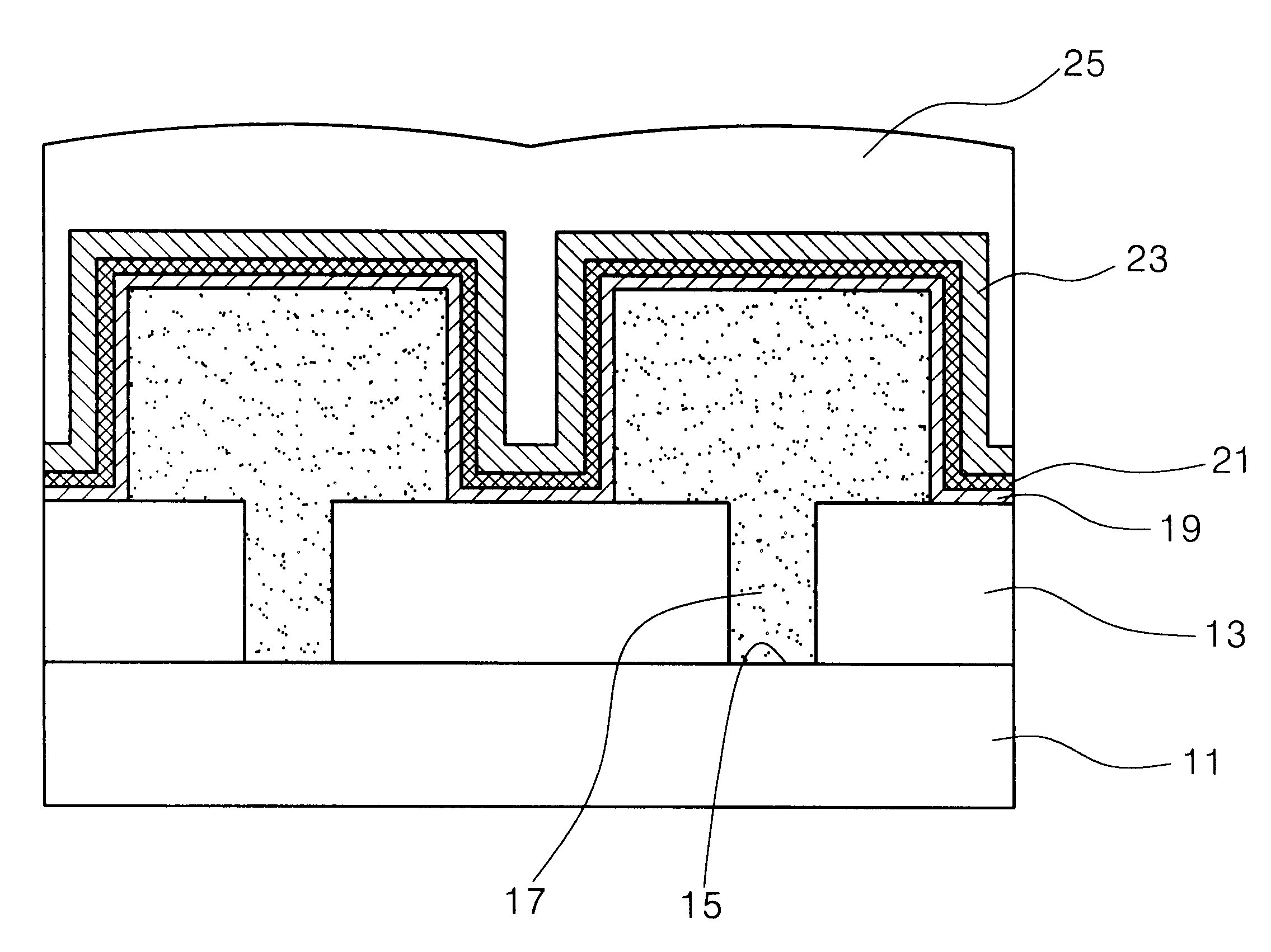
FIG. 2 is a cross-sectional view for illustrating a method for fabricating a capacitor of a semiconductor device in accordance with the present invention.

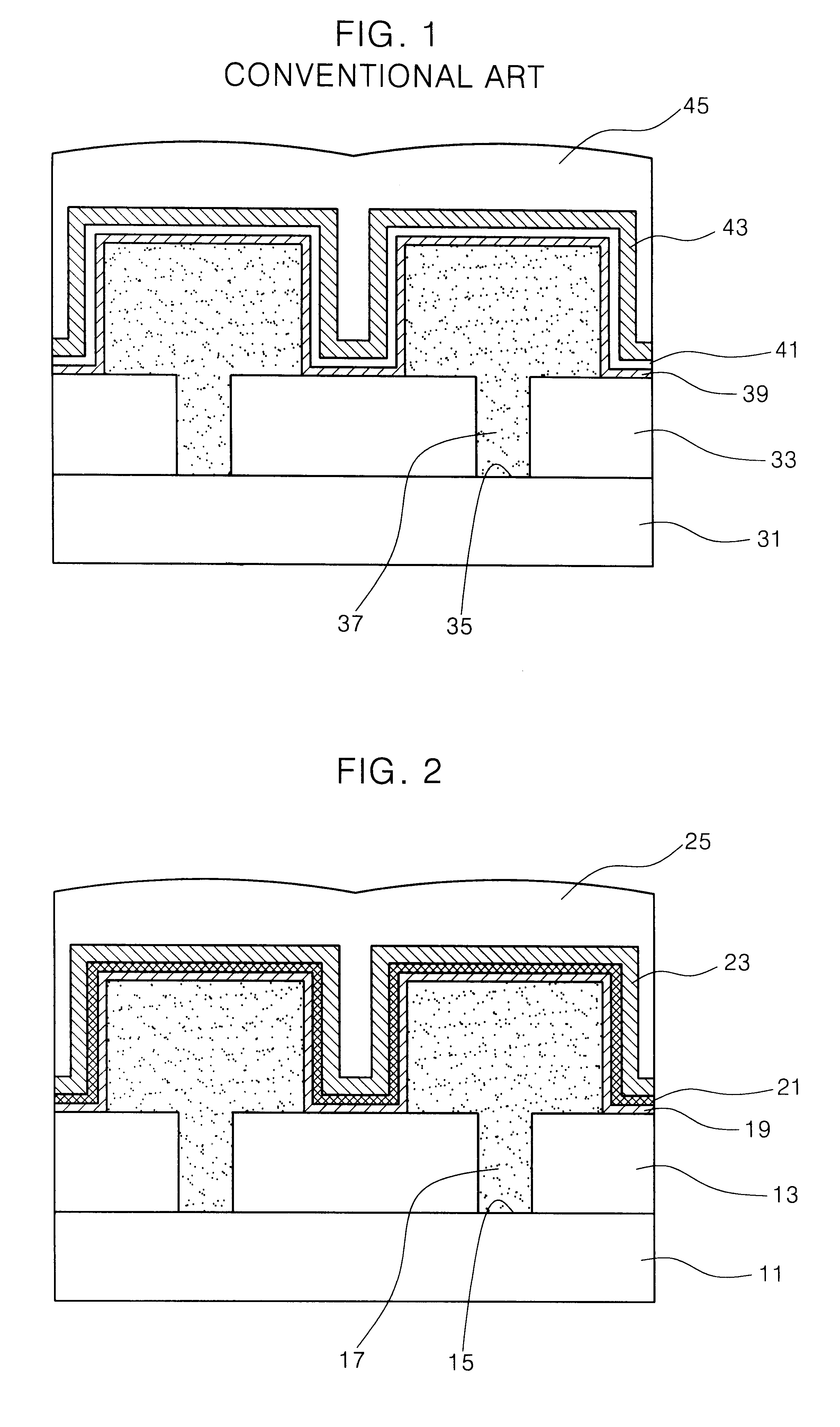
First of all, even if not shown in FIG. 1, a lower insulating layer 13 is constructed by forming device isolation insulating layer, gate oxide layer and gate electrode or bit line, and depositing BPSG on the substrate 11.

Then, a contact mask (not shown) is used for an etching process of forming storage nodes through contact holes 15 to expose an impurity diffusion region at predetermined portions of the substrate 11.

Accordingly, bottom electrode 17 is formed for being connected with predetermined portions of the substrate 11 through the contact holes 15.

At this time, the bottom electrode 17 can be made of silicon, conductivity oxide or metal layer. In this pre...


PUM


Abstract

The invention relates to a method for fabricating a capacitor of a semiconductor device including the steps of: forming storage nodes for being connected with predetermined portions of a semiconductor substrate; forming a surface nitride layer by performing a surface nitrification process for preventing formation of an oxide layer on the surface of the storage nodes that deteriorates dielectric characteristic of the layer; forming an alumina (Al2O3) layer as a dielectric layer on the surface nitride layer in a perovskite structure with superior electrical and mechanical strength; and forming a plate electrode on the dielectric layer, thereby forming a capacitor with capacitance high enough to achieve high integration of the semiconductor device.

Description

1. Field of the InventionThe present invention relates to a method for fabricating a semiconductor device, and more particularly to a method for fabricating a capacitor of a semiconductor device having a dielectric layer with higher dielectric characteristic than a conventional nitride / oxide deposition structure of a dielectric layer by forming an alumina (A203) layer in a perovskite structure (Al+B5+O3) of superior electrical and mechanical strength.2. Description of the Prior ArtAs integration of a semiconductor memory device gets higher, the size of cells gets smaller. Therefore, it is more and more difficult to secure sufficient capacitance that is in proportion to the surface area of storage nodes.Particularly, in case of a DRAM device constructed with one MOS transistor and capacitor in a unit cell, it is a key factor for high integration of a DRAM device to reduce the size of a chip while capacitance of a capacitor, occupying a large area of a chip, is kept large.Thus, in ord...

Claims


Application Information

Patent Timeline
IPC IPC(8): H01L21/02H01L21/314H01L21/316H01L27/04H01L27/108
CPCH01L21/02178H01L21/02271H01L21/02304H01L28/56H01L21/02356H01L21/3144H01L21/3162H01L21/02337H01L27/04H10B12/00
Inventor LEE, KEE-JEUNG
Owner INTELLECTUAL DISCOVERY CO LTD
Why Eureka
Try Eureka