Field effect semiconductor device

a semiconductor device and field effect technology, applied in the field of field effect transistors, can solve problems such as free electron leakage below, and achieve the effect of higher resistan

Inactive Publication Date: 2002-03-12
MITSUBISHI ELECTRIC CORP
View PDF13 Cites 28 Cited by
  • Summary
  • Abstract
  • Description
  • Claims
  • Application Information

AI Technical Summary

Benefits of technology

A first field effect transistor device according to the invention comprises a channel layer made of a compound semiconductor, a first compound semiconductor layer formed below the channel layer and having a higher resistance than the channel layer, and a second compound semiconductor layer formed below the first compound semiconductor layer and facilitating re-combination of carriers.

Problems solved by technology

However, even if the characteristics of the channel layer is improved, free electrons leak below the channel due to short channel effect because a very small gate electrode has to be used.

Method used


Image

  • Field effect semiconductor device
  • Field effect semiconductor device
  • Field effect semiconductor device

Examples


second embodiment

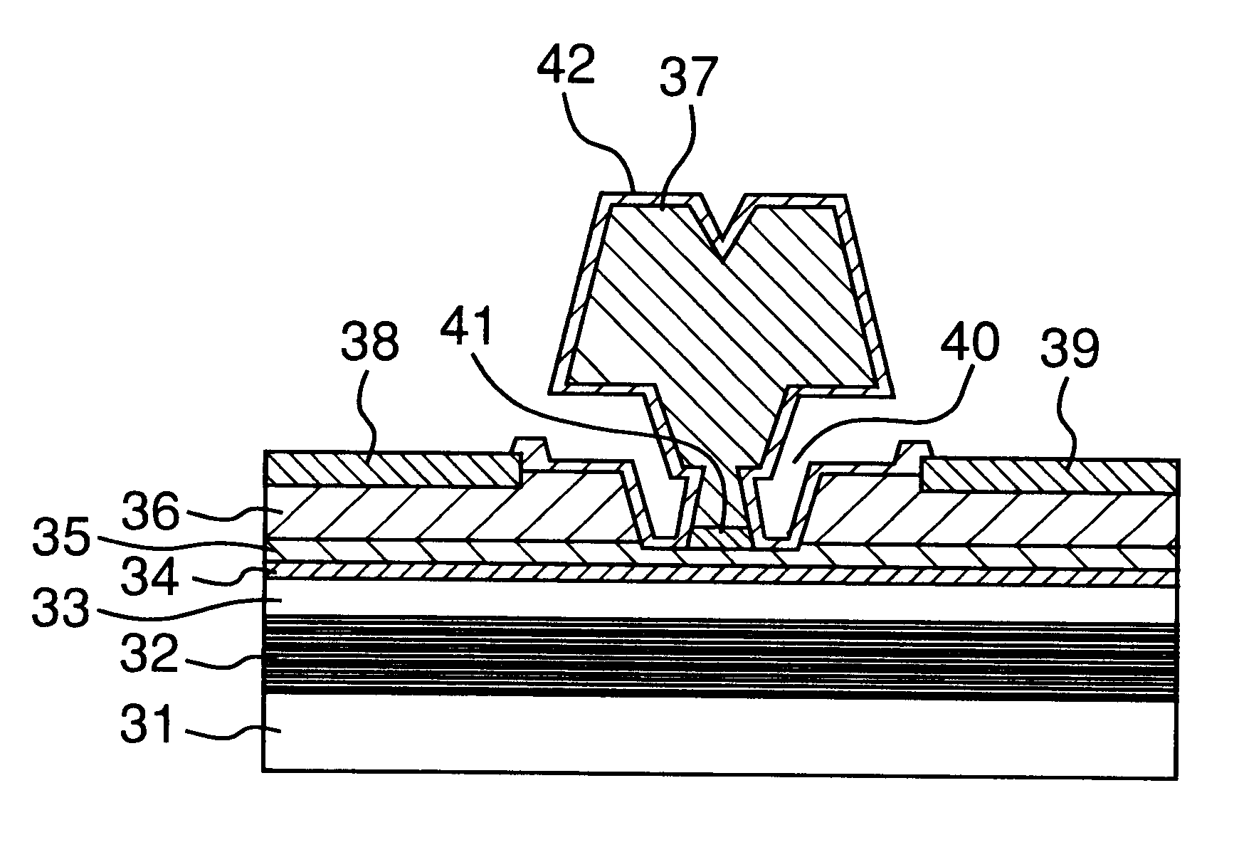
FIG. 5 is a schematic diagram of a GaAs low noise FET (HEMT) according to the invention. On a semi-insulating GaAs substrate 31, a superlattice buffer layer 32 is fabricated by forming 40 layers wherein AlGaAs layers mixed with 2*10.sup.17 cm.sup.-3 of oxygen (of thickness of 15 nm) and GaAs layers (of thickness of 5 nm) are formed alternately. An undoped GaAs layer 33 (of thickness of 300 nm) and an undoped InGaAs channel layer 34 are formed on the superlattice layer 32. On the channel layer 34, an n-AlGaAs layer 35 and an n.sup.+ -GaAs layer 36 are formed further. A recess groove 40 is formed at the center of the n.sup.+ -GaAs layer 36, and a gate electrode 37 is formed at the center of the recess groove 40. In order to improve the Schottky junction, a TiAl layer 41 is formed between the gate electrode 37 and the n-AlGaks layer 35. Further, a source electrode 38 and a drain one 39 are formed on the n.sup.+ -GaAs layer 36 at both sides with respect to the recess groove 40. A passiv...

first embodiment

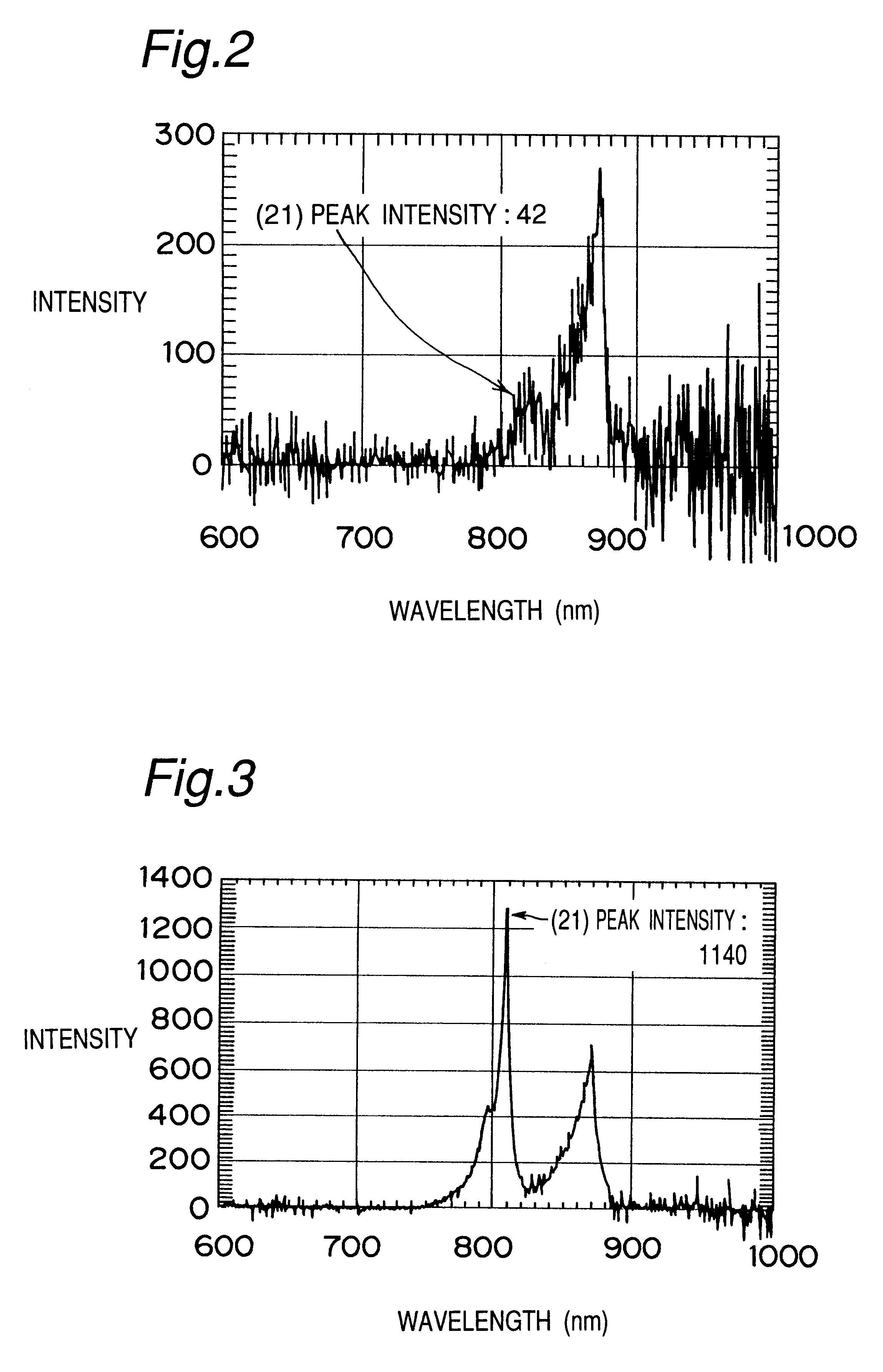
FIGS. 12 to 15 show measurement data of photoluminescence for explaining an effect of low temperature growth. FIGS. 12 and 13 show comparison data when the superlattice buffer layer is grown at the conventional growth temperature (T.sub.g =560.degree. C.). FIG. 12 shows measurement data when the oxygen concentration in the AlGaAs layer in the superlattice buffer layer is smaller than 2*10.sup.16 cm.sup.-3, and FIG. 13 shows measurement data when the oxygen concentration is smaller than 1*10.sup.17 cm.sup.-3 (in correspondence to the first embodiment). On the other hand, FIGS. 14 and 15 show measurement data when the oxygen concentration in the AlGaAs layer is smaller than 2*10.sup.16 cm.sup.-3 and when the growth temperature of the superlattice buffer layer is lower by 100.degree. C. and by 200.degree. C., respectively, than the cases shown in FIGS. 12 and 13. It is apparent that the data shown in FIG. 14 has the peak intensity decreased to about a half of the data shown in FIG. 12 ...


PUM


Abstract

In a field effect transistor such as high output FET or low noise HEMT, a layer for facilitating re-combination of carriers (for example a superlattice buffer layer), an undoped compound semiconductor layer having a higher resistance than a channel layer and the channel layer made of a compound semiconductor are layered successively. In the layer for facilitating re-combination of carriers, for example, oxygen of high concentration is introduced, to facilitate the non-radiative recombination which shortens the life of injected carriers. The layer for facilitating re-combination of carriers is also formed by forming the superlattice layer at a lower temperature than the channel layer. Thus, efficiency and voltageproofness on high frequency, high output power operation is improved further, and noises can be decreased further on high frequency, low noise operation.

Description

This application is the national phase under 35 U.S.C. .sctn.371 of PCT International Application No. PCT / JP97 / 02559 which has an International filing date of Jul. 24, 1997, which designated the United States of America.1. Technical FieldThe present invention relates to a field effect transistor, in particular, to a device structure of compound semiconductor field effect transistor for realizing higher efficiency and higher voltageproofness in high frequencies, and high output power operation and for realizing lower noises in high frequency, low noise operation.2. Background ArtDevices made of a compound semiconductor such as GaAs have been used in various uses not realized by silicon devices. A superlattice structure wherein GaAs and AlGaAs very thin films are grown in layers is also used in compound semiconductor devices. Devices using superlattice structure include a high output power field effect transistor (FET) and a low noise high mobility transistor (HEMT). The superlattice ...

Claims


Application Information

Patent Timeline
Patent Type & Authority Patents(United States)
IPC IPC(8): H01L29/02H01L21/02H01L21/335H01L21/285H01L21/338H01L29/15H01L29/10
CPCH01L21/28587H01L29/1075H01L29/66871H01L29/66462H01L29/155
Inventor HATTORI, RYO
Owner MITSUBISHI ELECTRIC CORP
Why Eureka
Try Eureka