Gallium nitride-based compound semiconductor laser and method of manufacturing the same

a gallium nitride and compound semiconductor technology, applied in semiconductor lasers, semiconductor laser structural details, lasers, etc., can solve the problems of low efficiency of carrier injection into the active layer, inability to obtain high-quality crystals, and inability to obtain satisfactory laser characteristics, etc., to achieve low voltage, high reliability, and suppress voltage drop

Inactive Publication Date: 2002-03-19
KK TOSHIBA
View PDF12 Cites 33 Cited by
  • Summary
  • Abstract
  • Description
  • Claims
  • Application Information

AI Technical Summary

Benefits of technology

The present invention has been made in consideration of the above situations, and has as its object to provide a highly reliable gallium nitride-based compound semiconductor laser which allows efficient injection of carriers into the active layer, can suppress voltage drops at the electrode contacts and the like, is used for optical disks and the like, and operates at a low threshold and a low voltage, and a method of manufacturing the same.

Problems solved by technology

In either of these proposed techniques, a laser having satisfactory characteristics has not been obtained because a gallium nitride-based compound semiconductor layer is difficult to cause crystal growth.
That is, even if a gallium nitride-based compound semiconductor layer is formed by crystal growth, a high-quality crystal cannot be obtained.
Since the crystal quality is poor, carriers cannot be efficiently injected into the active layer.
In addition, in a structure having a striped opening in a current blocking layer, the crystal quality of the regrown layer formed after etching for forming the striped opening deteriorates, resulting in voltage drops at the electrode contacts and the like.
However, with the prior techniques, these requirements cannot be satisfied.
According to a semiconductor laser using a gallium nitride-based compound semiconductor material, it is difficult to cause crystal growth of the material and to obtain a high-quality crystal layer.
In addition, the crystal quality of the regrown layer formed after etching for forming a striped opening deteriorates.
For these reasons, carriers cannot be efficiently injected into the active layer, and voltage drops occur at the electrode contacts and the like.
That is, it is difficult to realize a highly reliable device which is used for optical disks and the like and operates at a low threshold and a low voltage.

Method used


Image

  • Gallium nitride-based compound semiconductor laser and method of manufacturing the same
  • Gallium nitride-based compound semiconductor laser and method of manufacturing the same
  • Gallium nitride-based compound semiconductor laser and method of manufacturing the same

Examples


Embodiment Construction

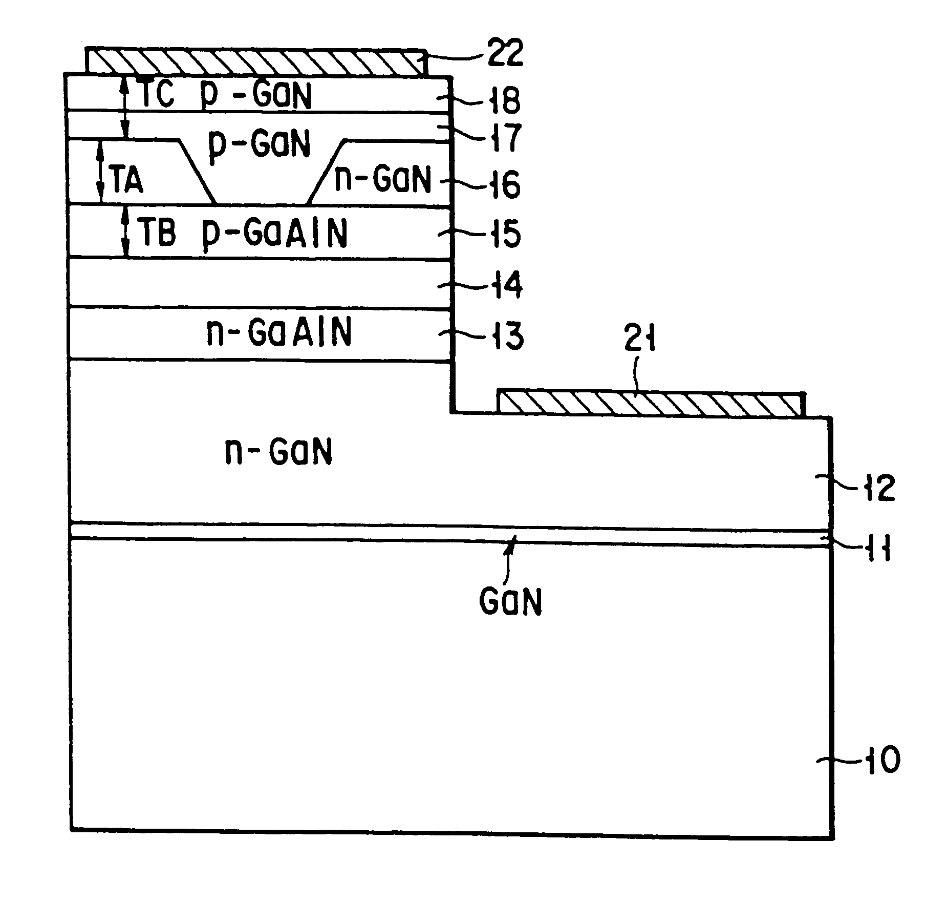
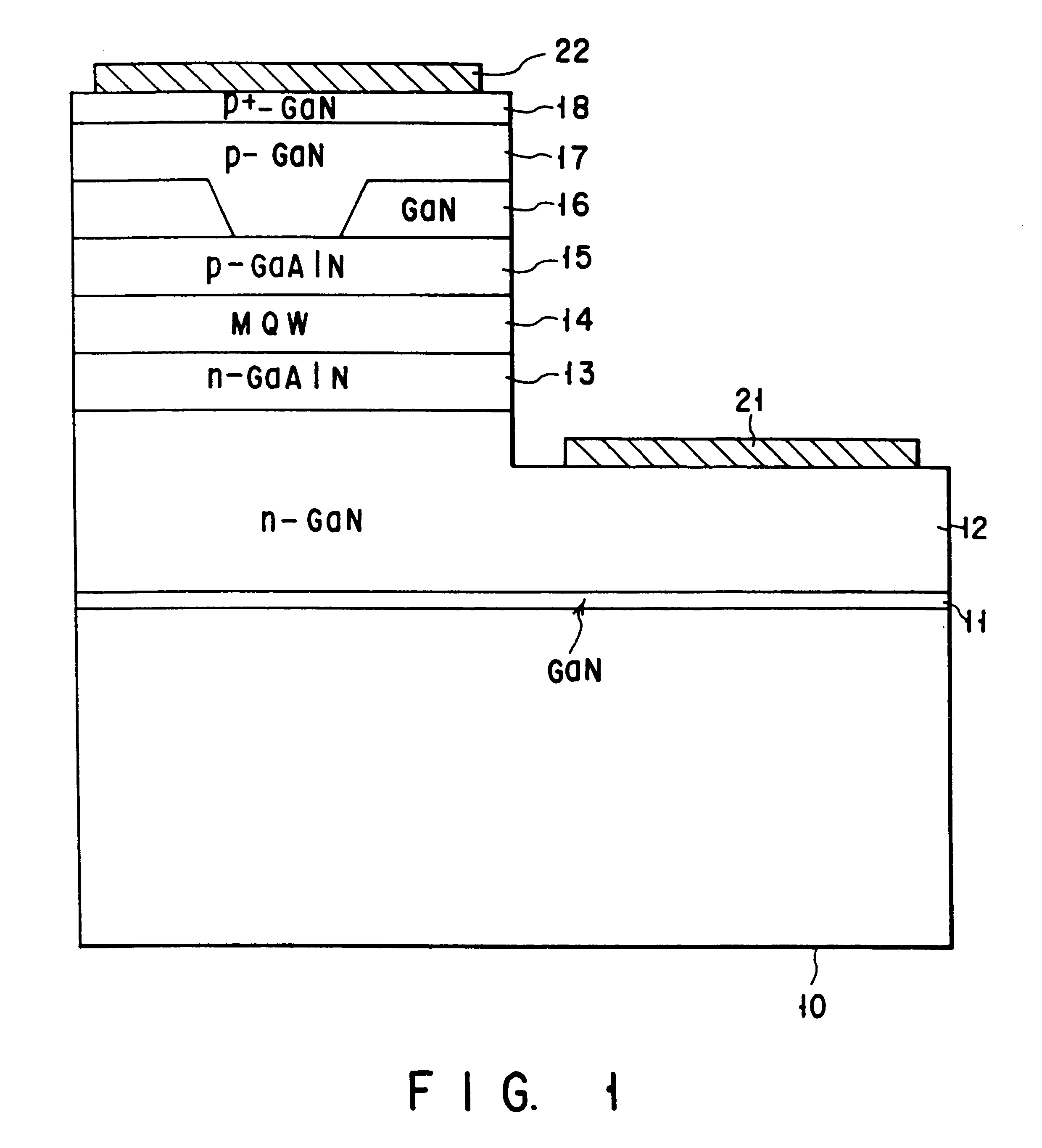
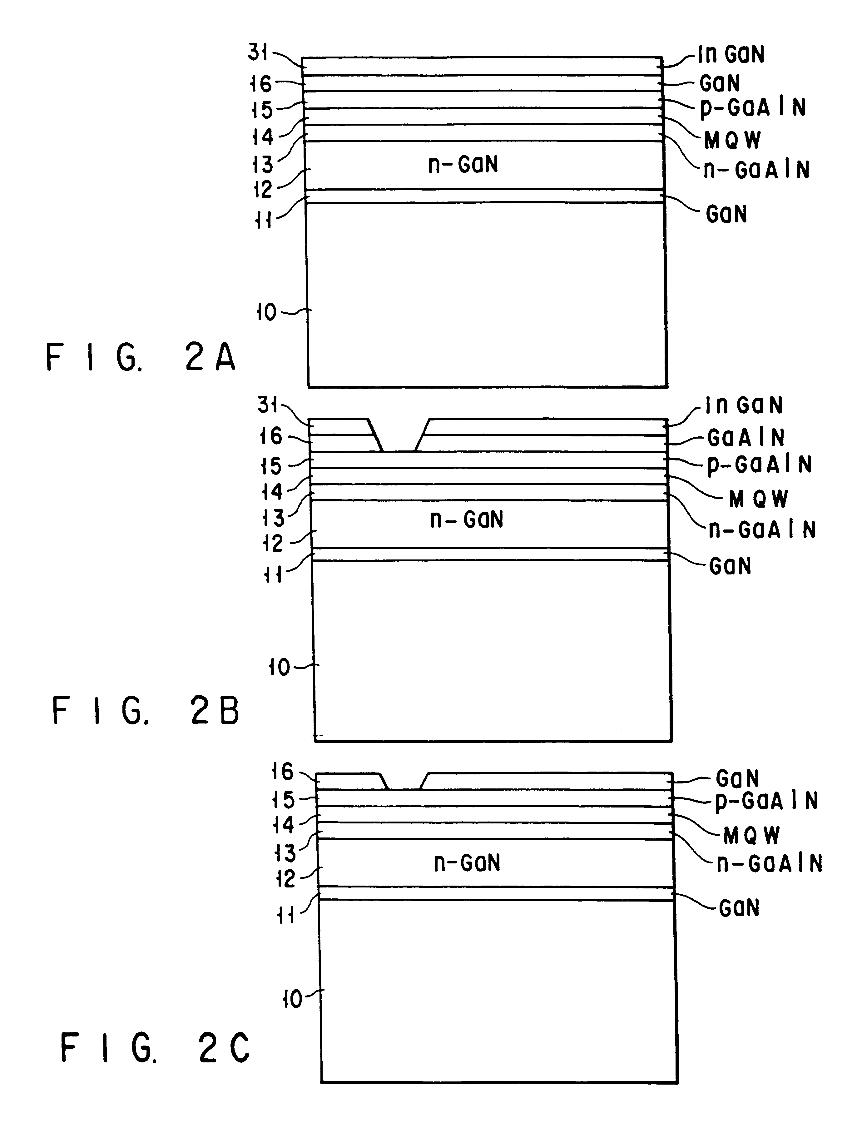
FIG. 1 is a sectional view showing the structure of a gallium nitride-based compound semiconductor laser according to an embodiment of the present invention. The same reference numerals denote parts having substantially the same functions and arrangements in the following description, and a repetitive description thereof will be made as needed.

A GaN buffer layer 11, a GaN buffer layer 11, an Si-doped n-GaN contact layer 12, an Si-doped n-GaAlN cladding layer 13, an MQW active layer 14, an Mg-doped p-GaAlN cladding layer 15, and an undoped GaN current blocking layer 16 are stacked on a sapphire substrate 10. The GaN current blocking layer 16 is etched in the form of a stripe. The MQW active layer 14 has a multiple quantum well (MQW) structure having a cyclic structure formed by cyclically stacking two types of InGaAlN layers which are different in band gap energy and 10 nm or less thick.

An Mg-doped p-GaN buried layer 17 and an Mg-doped p.sup.+ -GaN contact layer 18 are stacked on a p...


PUM


Abstract

A gallium nitride-based compound semiconductor laser has a double-heterojunction structure, in which an active layer is sandwiched between cladding layers, on a sapphire substrate. A GaN current blocking layer having a striped opening portion is formed on the p-cladding layer. A p-GaN buried layer and a contact layer through which a current is injected into the opening portion of the current blocking layer and which are larger in area than the opening portion are formed. The active layer has a multiple quantum well structure constituted by a cyclic structure formed by cyclically stacking two types of InGaAlN layers which have different band gaps and are 10 nm or less thick.

Description

BACKGROUND OF THE INVENTIONThe present invention relates to a semiconductor device using a gallium nitride-based compound semiconductor and a manufacturing technique for the same and, more particularly, to a gallium nitride-based compound semiconductor laser, a method of manufacturing the same, and a method of manufacturing a gallium nitride-based compound semiconductor device.In recent years, gallium nitride-based compound semiconductors such as GaN, InGaN, GaAlN, and InGaAlN have received a great deal of attention as materials for blue semiconductor lasers. Semiconductor lasers using these materials are designed as short-wavelength lasers and hence can focus beams to small diameters. Owing to this advantage, these lasers are expected to be used as light sources for high-density information processing such as processing in optical disks.Various structures and manufacturing methods have been proposed for semiconductor lasers of this type. In either of these proposed techniques, a la...

Claims


Application Information

Patent Timeline
Patent Type & Authority Patents(United States)
IPC IPC(8): H01S5/323H01S5/00H01S5/02H01S5/042H01S5/20H01S5/22H01S5/223H01S5/30H01S5/32H01S5/343
CPCB82Y20/00H01S5/2202H01S5/2231H01S5/32341H01S5/34333H01S2304/04H01S5/0421H01S5/0422H01S5/0425H01S5/2063H01S5/2205H01S5/2216H01S5/222H01S5/2224H01S5/2227H01S5/2232H01S5/3063H01S5/3211H01S5/3213H01S5/0213H01S5/04252H01S5/04257H01S5/2013H01S5/32325H01S5/32333
Inventor ISHIKAWA, MASAYUKIYAMAMOTO, MASAHIRONUNOUE, SHINYANISHIO, JOHJIHATAKOSHI, GENICHIFUJIMOTO, HIDETOSHI
Owner KK TOSHIBA
Why Eureka
Try Eureka