Method and system for modifying and densifying a porous film
a technology of porous film and densification method, which is applied in the direction of nuclear engineering, transportation and packaging, railway signalling, etc., can solve the problems of large time-consuming and laborious preparation of xerogels, small circuit layouts stacked in a multi-layer structure are susceptible to parasitic effects, and air does not lend itself to multi-layer design
- Summary
- Abstract
- Description
- Claims
- Application Information
AI Technical Summary
Benefits of technology
Problems solved by technology
Method used
Image

Examples
first embodiment
1. First Embodiment
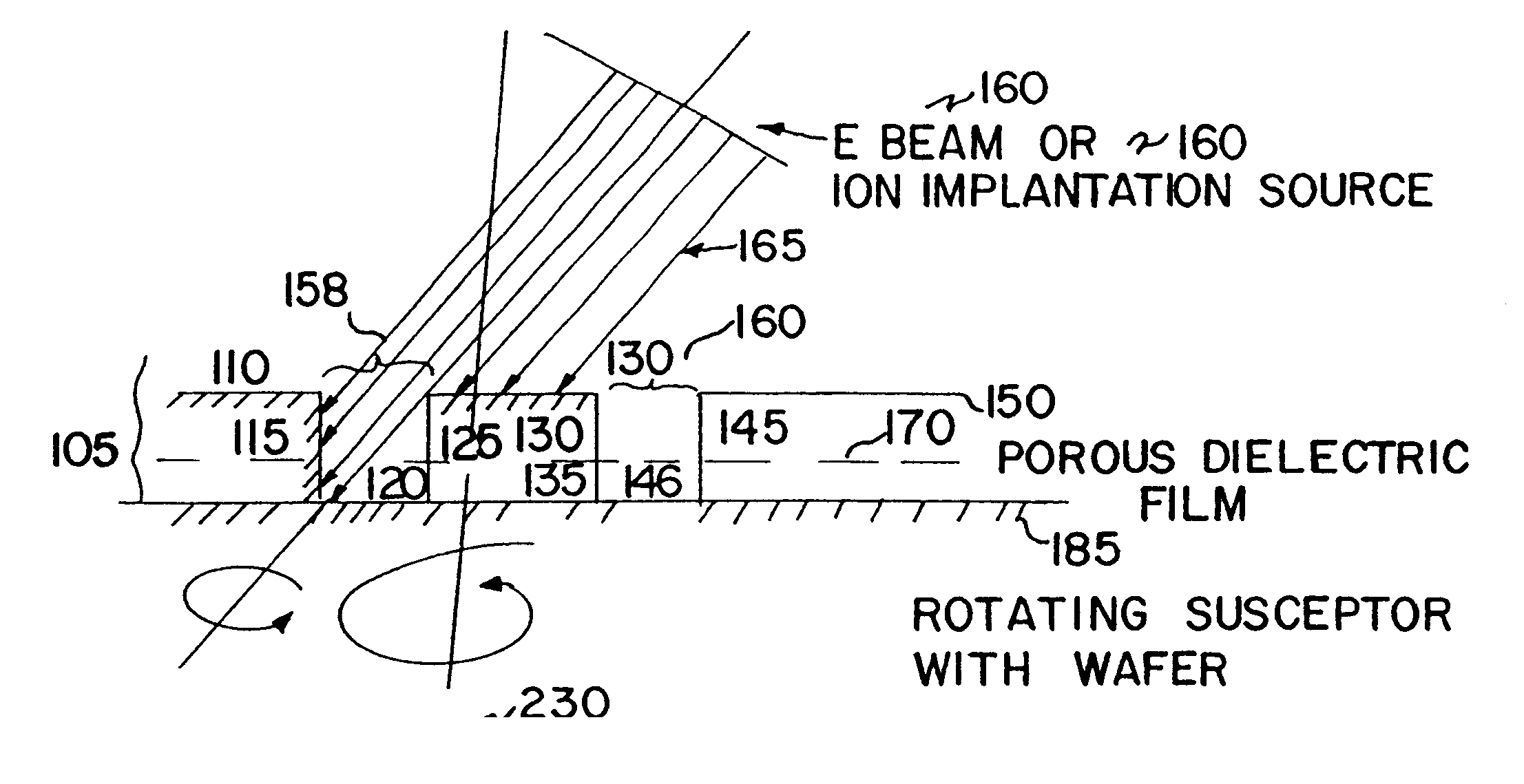
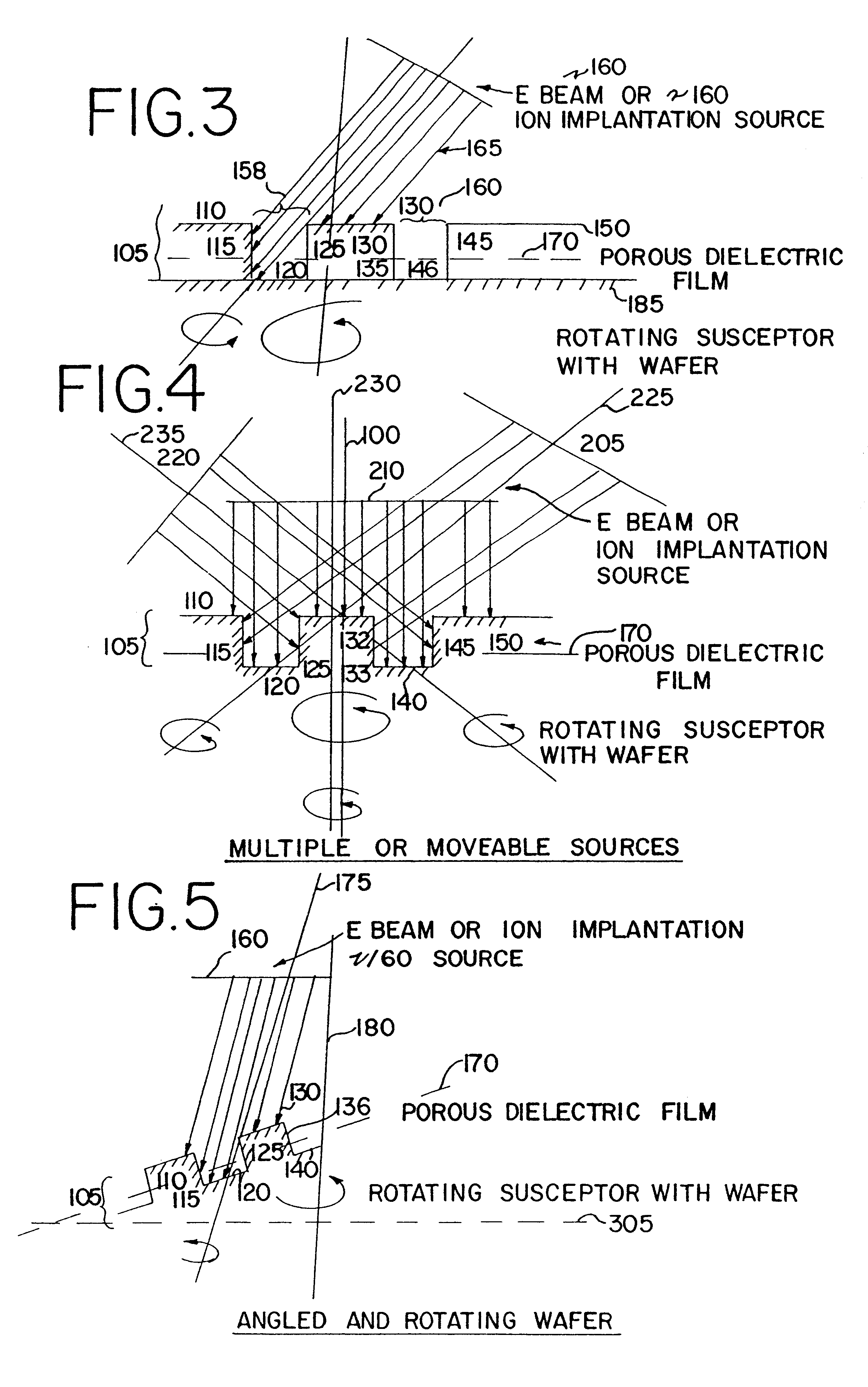
A tunable dielectric comprising the film 105 having a plurality of pores is shown in FIG. 3. Preferably, the film 105, which may be a thin film, is supported by an underlying structure 185, such as a semiconductor substrate with or without underlying process layers. Utilizing a radiation source 160 that can be rotated inclined, and / or moved, one or more electron beams 165 are formed. In a first embodiment, an "Electron Cure 30" manufactured by Allied Signal Incorporated of San Diego, Calif. provides the radiation source 160. The electron beams 165 preferably radiate along one 175 or more beam axes. When the thin film 105 is placed at a processing position 100, the electron beams 165 irradiate one or more select areas of the thin film 105. In FIG. 3, the select areas comprise the second side wall 115 and the second substantially plane surface 130. In these areas 115 and 130, the electron beams 165 preferably form an acute radiating angle between the beam axes 175 a...
second embodiment
2. Second Embodiment
FIG. 4 shows a second embodiment that also reduces the porosity of thin film 105. Only those parts of the second embodiment that are different from the first embodiment will be described. As shown, the exposed surfaces of thin film 105 are irradiated from three distinct sources of radiation 205, 210, and 220. The three sources 205, 210, and 220 that are shown are focused at specific surfaces 110, 115, 120, 125, 130, 135, 140, 145, and 150 that collectively comprise the exposed surface. The second embodiment allows for the rotation of the radiation sources 205, 210, and 220 and the thin film 105 about a plurality of beam axes 225, 230, and 235 and a rotational axis 180, respectively. Moreover, the second embodiment allows the radiation sources 205, 210, and 220 and the thin film 105 to be inclined through a plurality of angles measured between the level horizontal surface 305 (shown in FIG. 5) and the beam axes 225, 230, and 235 and the level horizontal surface an...
third embodiment
3. Third Embodiment
FIG. 5 depicts a modification of the first embodiment as it shows both a single movable radiation source 160 and illustrates the thin film 105 in an inclined and rotating state. As explained above, as the select areas of the thin film 105 are irradiated, the radiation source 160 and the thin film 105 are rotated to ensure even coverage of select areas 110, 115, 120, and 130. Likewise, the radiation source 160 and the thin film 105 may be inclined. Moreover, the rotation and the inclination of the radiation source 160 and the thin film 105 may continuously change, as the exposed surface is irradiated to ensure that the select areas 110, 115, 120, and 130 attain a predetermined dielectric constant.
Porous silica xerogels and aerogels were used as representative dielectric films in the above-described embodiments. However, those skilled in the art will appreciate that the invention envisions the use of other porous materials, such as, for example, materials that have ...
PUM
| Property | Measurement | Unit |
|---|---|---|
| thickness | aaaaa | aaaaa |
| thickness | aaaaa | aaaaa |
| dielectric constant | aaaaa | aaaaa |
Abstract
Description
Claims
Application Information
 - R&D
- Intellectual Property
- Life Sciences
- Materials
- Tech Scout
- Unparalleled Data Quality
- Higher Quality Content
- 60% Fewer Hallucinations
Browse by: Latest US Patents, China's latest patents, Technical Efficacy Thesaurus, Application Domain, Technology Topic, Popular Technical Reports.
© 2025 PatSnap. All rights reserved.Legal|Privacy policy|Modern Slavery Act Transparency Statement|Sitemap|About US| Contact US: help@patsnap.com