Field programmable gate array with mask programmed input and output buffers

a gate array and input buffer technology, applied in the field of integrated circuit input and output buffers, can solve the problems of increasing capacitance and resistive delay, new set of problems, and consuming time and money

Inactive Publication Date: 2002-03-26
ACTEL CORP
View PDF207 Cites 35 Cited by
  • Summary
  • Abstract
  • Description
  • Claims
  • Application Information

AI Technical Summary

Benefits of technology

It is another object of the present invention to optimize the functional capability of the input and output buffers of the integrated circuit die while minimizing the capacitance and resistive delay associated with the input and output buffer circuits.
It is a further object of the present invention to provide output buffers for an FPGA which inject less noise into the FPGA.
It is another object of the present invention to provide output buffers for an FPGA which have low power consumption.
According to the present invention, a mask programmed portion of an integrated circuit provides some of the input and output buffer functions to an FPGA portion of the integrated circuit to provide additional functional capability to the I / O buffers, and improves the flexibility, signal isolation, speed and power management of the FPGA architecture. In CMOS technology, the mask programmed portion comprises N-channel and P-channel MOS transistors that can be connected together to implement almost any type of I / O buffer function conceivable in CMOS technology.

Problems solved by technology

Further, when a variety of input or output functions is provided at each pin of the integrated circuit die, the logic function modules which are provided to implement functions which are not selected for a particular input or output pin add additional capacitance and resistive delay.
This solution, however, to the problems of additional capacitance and resistive delay simply raises a new set of problems.
The selection of a limited number of input and output buffer functions places constraints on the place and route algorithms used to implement the desired digital circuitry from the logic modules.
The development of placement and route routines which will optimize the use of the logic modules in the FPGA is an expensive and time consuming process.
Placing constraints on the functions which may be provided by the input and output buffers may not only substantially affect the utilization of the logic function modules, but, in a worst case, may keep the placement and routing algorithms from implementing the desired digital logic.
Finally, there are some input and output buffer functions that are desired, but cannot feasibly be implemented by logic function modules in an FPGA.

Method used


Image

  • Field programmable gate array with mask programmed input and output buffers
  • Field programmable gate array with mask programmed input and output buffers
  • Field programmable gate array with mask programmed input and output buffers

Examples


Embodiment Construction

Those of ordinary skill in the art will realize that the following description of the present invention is illustrative only and not in any way limiting. Other embodiments of the invention will readily suggest themselves to such skilled persons.

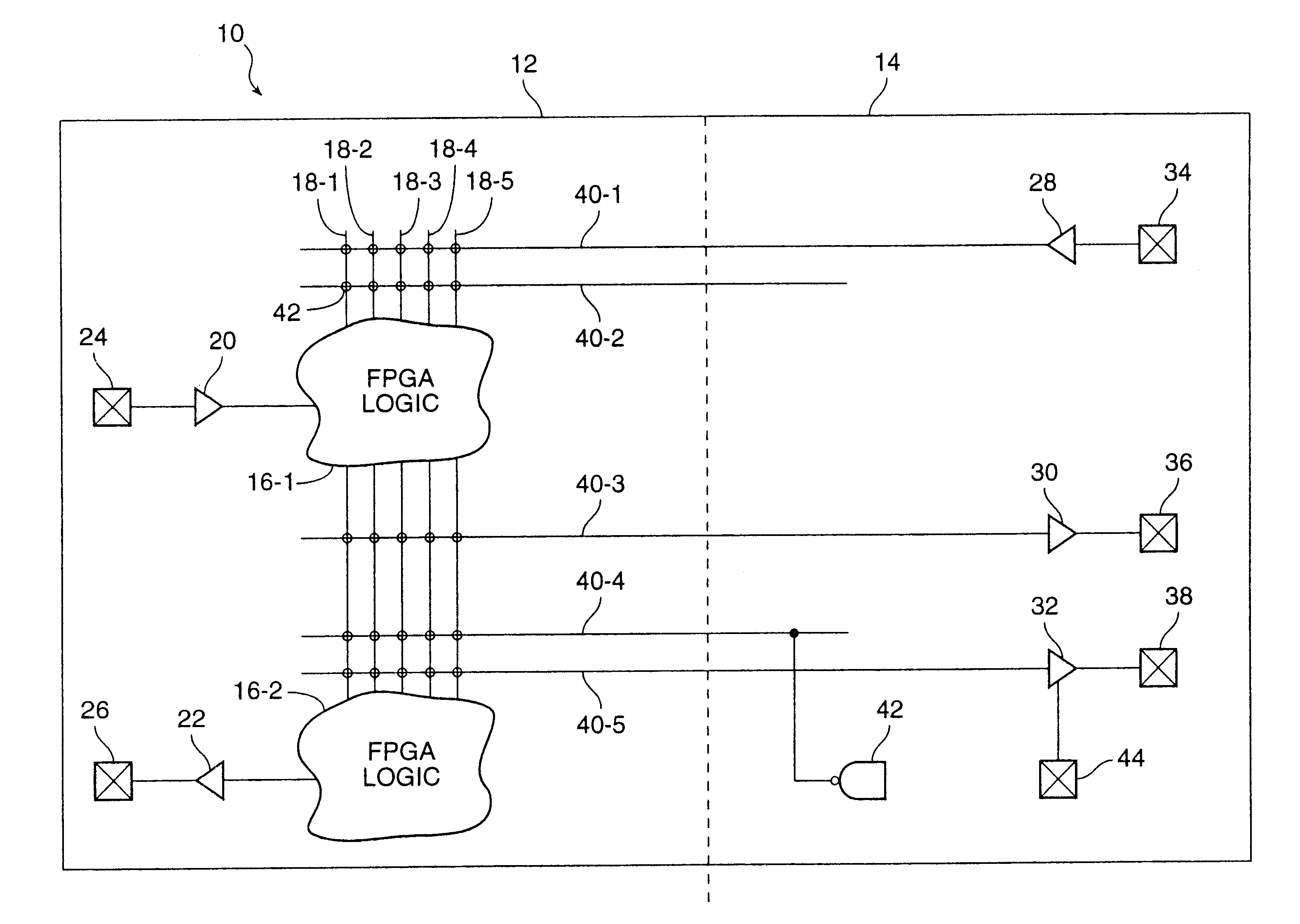
According to the present invention, a mask programmed (i.e., dedicated) portion of an integrated circuit provides some of the input and output (I / O) buffer functions to an FPGA portion of the integrated circuit. Conventionally all the I / O buffer functions of an FPGA are provided by I / O buffers configured by inputs from the logic modules of the FPGA. Mask programming some of the I / O buffer functions in an FPGA provides additional functional capability to the I / O buffers. In CMOS technology, the mask programmed portion comprises N-channel and P-channel MOS transistors that can be connected together to implement almost any type of I / O buffer function conceivable in CMOS technology. It should be appreciated that technologies other than CMOS are a...


PUM


Abstract

A hybrid integrated circuit architecture comprising a mask programmable portion and a field programmable gate array portion. The mask programmable portion has a plurality of mask programmed input and output buffer circuits, and a first group of input / output pads, wherein one of the input / output pads of the first group is connected to an input of one of the input buffer circuits, and one of the input / output pads of the first group is connected to an output of one of the output buffer circuits. The field programmable gate array portion has programmable digital logic function modules, a second group of input / output pads, interconnect conductors divided into one or more segments, wherein some segments run in a first direction and some segments run in a second direction to form intersections and some segments form intersections with inputs and outputs of the digital logic function modules, the first group of input / output pads, and inputs and outputs of the output and input buffer circuits from the mask programmable portion, and user programmable interconnect elements connected between adjoining ones of the segments in a same one of the interconnect conductors, and between intersections of selected ones the first and second segments, intersections of inputs and outputs of the digital logic function modules and selected interconnect conductors, intersections of the first group of input / output pads and selected ones of the interconnect conductors, intersections with outputs of the input buffer circuits and selected ones of the interconnect conductors, and intersections with the inputs of the output buffer circuits and selected ones of the interconnect conductors.

Description

1. Field of the InventionThe present invention relates to input and output buffers in an integrated circuit. More particularly, the present invention relates an integrated circuit having a field programmable gate array (FPGA) portion and a mask programmable portion, wherein the mask programmable portion provides specialized input and output buffer functions to the integrated circuit.2. The Prior ArtIn an integrated circuit die, signals are transferred into and out of the die by input and output buffers, respectively, configured as part of the integrated circuit within the die. The input and output buffers generally perform relatively standard functions that are useful on all inputs and outputs, however, any or all the input and output buffers may also be configured to perform a variety of specialized functions including voltage gain, current gain, level translation, delay, signal isolation or hysteresis.As is well known in the art, an FPGA is a collection of groups of gates partitio...

Claims


Application Information

Patent Timeline
Patent Type & Authority Patents(United States)
IPC IPC(8): H03K19/177
CPCH03K19/17788
Inventor MCGOWAN, JOHN E.
Owner ACTEL CORP
Why Eureka
Try Eureka