Silicon trench etch using silicon-containing precursors to reduce or avoid mask erosion

Inactive Publication Date: 2002-04-30
APPLIED MATERIALS INC
View PDF28 Cites 69 Cited by
  • Summary
  • Abstract
  • Description
  • Claims
  • Application Information

AI Technical Summary

Problems solved by technology

A deposition mode takes place when a particularly high concentration of the SC compound is used and/or a particularly high plasma source p

Method used


Image

  • Silicon trench etch using silicon-containing precursors to reduce or avoid mask erosion
  • Silicon trench etch using silicon-containing precursors to reduce or avoid mask erosion
  • Silicon trench etch using silicon-containing precursors to reduce or avoid mask erosion

Examples


example two

The Prior Art Single Step Etch Chemistry and Method

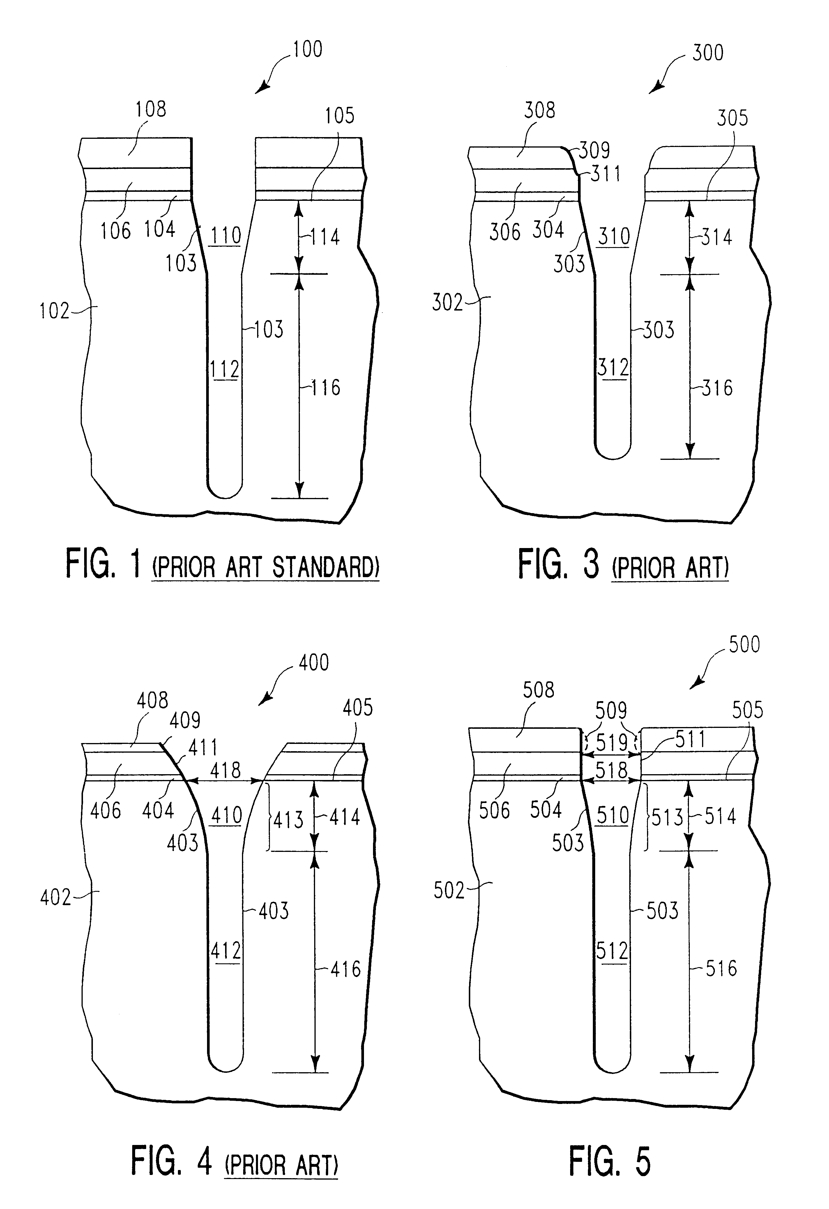
FIG. 4 illustrates a schematic of the cross-sectional profile of a deep etched silicon trench structure 400 obtained by applicants using a single step process of the kind previously known in the art. It was this single step process which was improved upon by applicants in the two step etch process described above in Example One. This example is provided for comparative purposes only.

In particular, the thickness of the borosilicate glass patterning mask 408 after etching of silicon trench 403 was about 1,800 .ANG.; the thickness of silicon nitride masking layer 406 remained at about 2,200 .ANG.; the thickness of pad oxide dielectric layer 404 was about 80 .ANG.. (FIG. 4 is not to scale.) The top portion 410 of the trench 403, which extends from the silicon surface 405 into the silicon substrate 402 a depth 414 of about 1.5 .mu.m is tapered at an angle of about 88.5.+-.0.2.degree.. As a result of the lateral erosion (as illustrated at...

example three

The Single Step Etch Chemistry and Method of the Present Invention

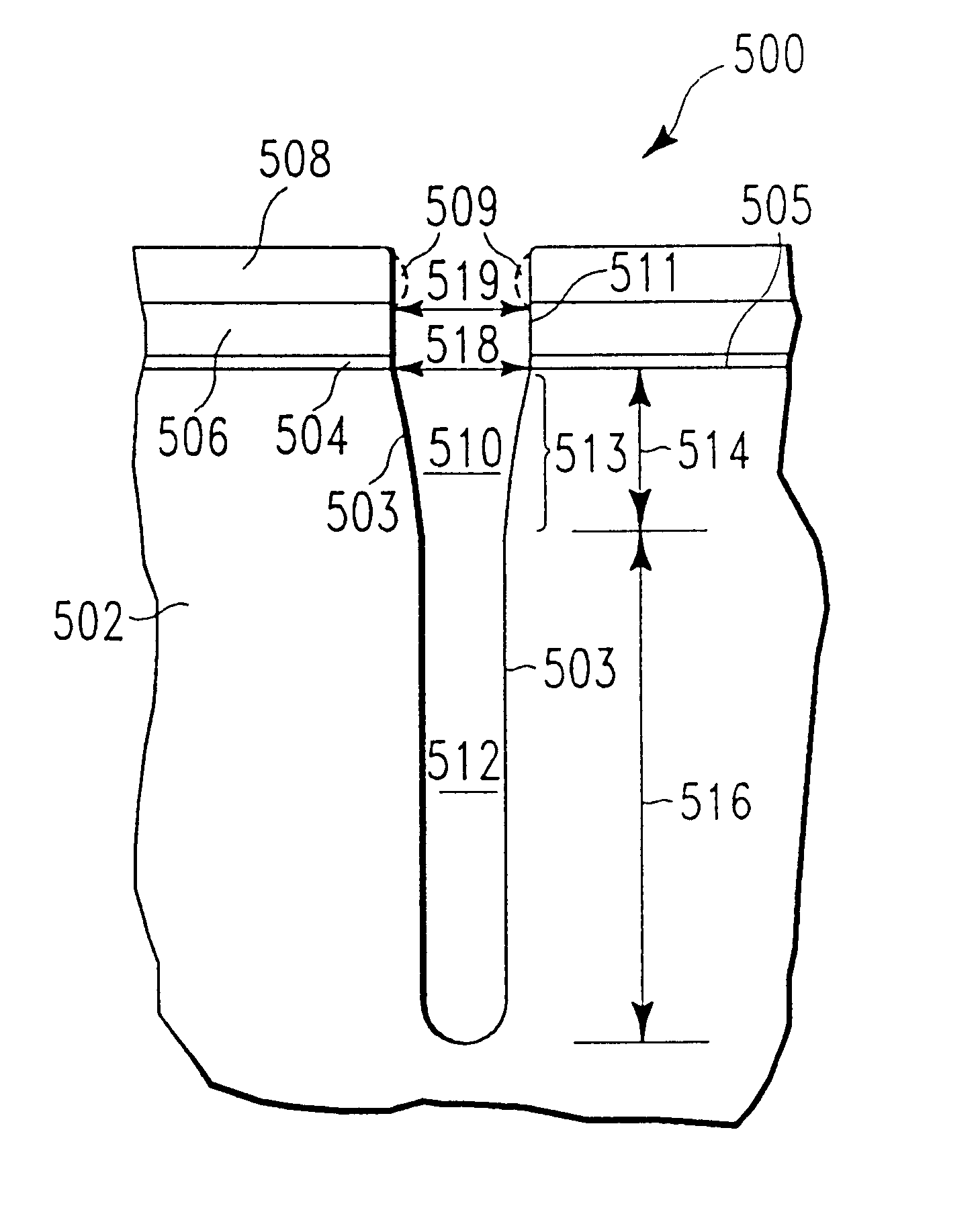
FIG. 5 illustrates a schematic of the cross-sectional profile of a deep etched silicon trench structure 500 obtained in a single etch step using the etch chemistry and method of the present invention.

In particular, the thickness of the borosilicate glass patterning mask 508 after etching of silicon trench 503 was about 5,600 .ANG.; the thickness of silicon nitride masking layer 506 remained at about 2,200 .ANG.; the thickness of pad oxide dielectric layer 504 was about 80 .ANG.. (FIG. 5 is not to scale.) The top portion 510 of the trench 503, extended from the silicon surface 505 into the silicon substrate 502 a depth 514 of about 1.5 .mu.m was tapered at an angle of 88.5.degree..+-.0.5.degree.. The critical dimension 518 was 0.32 .mu.m, which was maintained during etching because silicon nitride masking layer 506 maintained a constant dimension (as shown on the drawing at 519). The bottom portion 512 of the trench 50...

example four

Use of the First Step Etch Chemistry from the Prior Art and the Method of the Present Invention as the Second Step in a Two Step Process

FIG. 6 illustrates a schematic of the cross-sectional profile of a deep etched silicon trench structure 600 obtained by applicants using a two step process of the kind described in U.S. application Ser. No. 08 / 985,771, but substituting the etch chemistry and method of the present invention for the second step in the two step process.

In particular, the thickness of the borosilicate glass patterning mask 608 after etching of silicon trench 603 was about 5,900 .ANG.; the thickness of silicon nitride masking layer 606 remained at about 2,200 .ANG.; the thickness of pad oxide dielectric layer 604 was about 80 .ANG.. (FIG. 6 is not to scale.) The top portion 610 of the trench 603, which extended from the silicon surface 605 into the silicon substrate 602 a depth 614 of about 1.5 .mu.m was tapered at an angle of 88.4.+-.0.3.degree.. The critical dimension ...


PUM


Abstract

The present invention pertains to an etch chemistry and method useful for the etching of silicon surfaces. The method is particularly useful in the deep trench etching of silicon where profile control is important. In the case of deep trench etching, at least a portion of the substrate toward the bottom of the trench is etched using a combination of reactive gases including a fluorine-containing compound which does not contain silicon (FC); a silicon-containing compound (SC) which does not contain fluorine; and oxygen (O2).

Description

1. Field of the InventionThe present invention pertains to the plasma etching of silicon substrates. The method of the invention is generally applicable to the etching of silicon, but is particularly useful in the etching of deep trenches. A typical deep trench would have a diameter of about 0.15 .mu.m (or larger) and an aspect ratio as high as about 35:1. Silicon deep trench etching is most commonly used in capacitor technology and in particular in DRAM applications. Other potential applications for the present etching method include the etching of shallow trenches (currently having a typical feature size of about 0.25 .mu.m to about 0.4 .mu.m and an aspect ratio of about 1.1 to 2:1) used in applications such as device isolation; the etching of polysilicon gates; and, the etching of silicide layers. In addition, the present etching method is useful for the micro machining of silicon surfaces for biomedical applications, for example. The present method of plasma etching may be used ...

Claims


Application Information

Patent Timeline
IPC IPC(8): H01L21/02H01L21/3065
CPCH01L21/3065
Inventor LIU, WEIWANG, YIQIONGLI, MAOCHENGKHAN, ANISULPAN, SHAOHERPODLESNIK, DRAGAN
Owner APPLIED MATERIALS INC
Why Eureka
Try Eureka