Electron emission device with electron supply layer having reduced resistance

a technology of electron supply layer and electron supply layer, which is applied in the manufacture of electric discharge tube/lamp, tubes with screens, discharge tubes luminescnet screens, etc., can solve the problems of low production yield, insufficient electron emission of structure, and inferior electron emission characteristic of device, etc., and achieve high speed and improved production yield

Inactive Publication Date: 2002-05-14
PIONEER CORP
View PDF4 Cites 22 Cited by
  • Summary
  • Abstract
  • Description
  • Claims
  • Application Information

AI Technical Summary

Benefits of technology

According to the electron emission device of the invention with the above structure, the device comprises an electron-supply layer made of semiconductor, particularly elements belonging to group IV and having an additive of at least one material selected from atomic elements belonging to group III or V in the periodic table such as boron (B), phosphorus (P), to arsenic (As), antimony (Sb) and so on. Therefore, even when the plural electron emission devices used in a flat panel display device are subjected to a high temperature atmosphere in the manufacturing process, the devices can keep their properties before and after the heating treatment without thermal deterioration due to the high tempe...

Problems solved by technology

This FED, however, has a problem of low production yield because the manufacture of the minute Spindt-type emitter arrays as a cold cathode is complex and involves many processes.
However, even the electron emission device with the MIM stru...

Method used


Image

  • Electron emission device with electron supply layer having reduced resistance
  • Electron emission device with electron supply layer having reduced resistance
  • Electron emission device with electron supply layer having reduced resistance

Examples


Embodiment Construction

An electron emission device according to an embodiment of the present invention will be described in more detail with reference to the accompanying drawings.

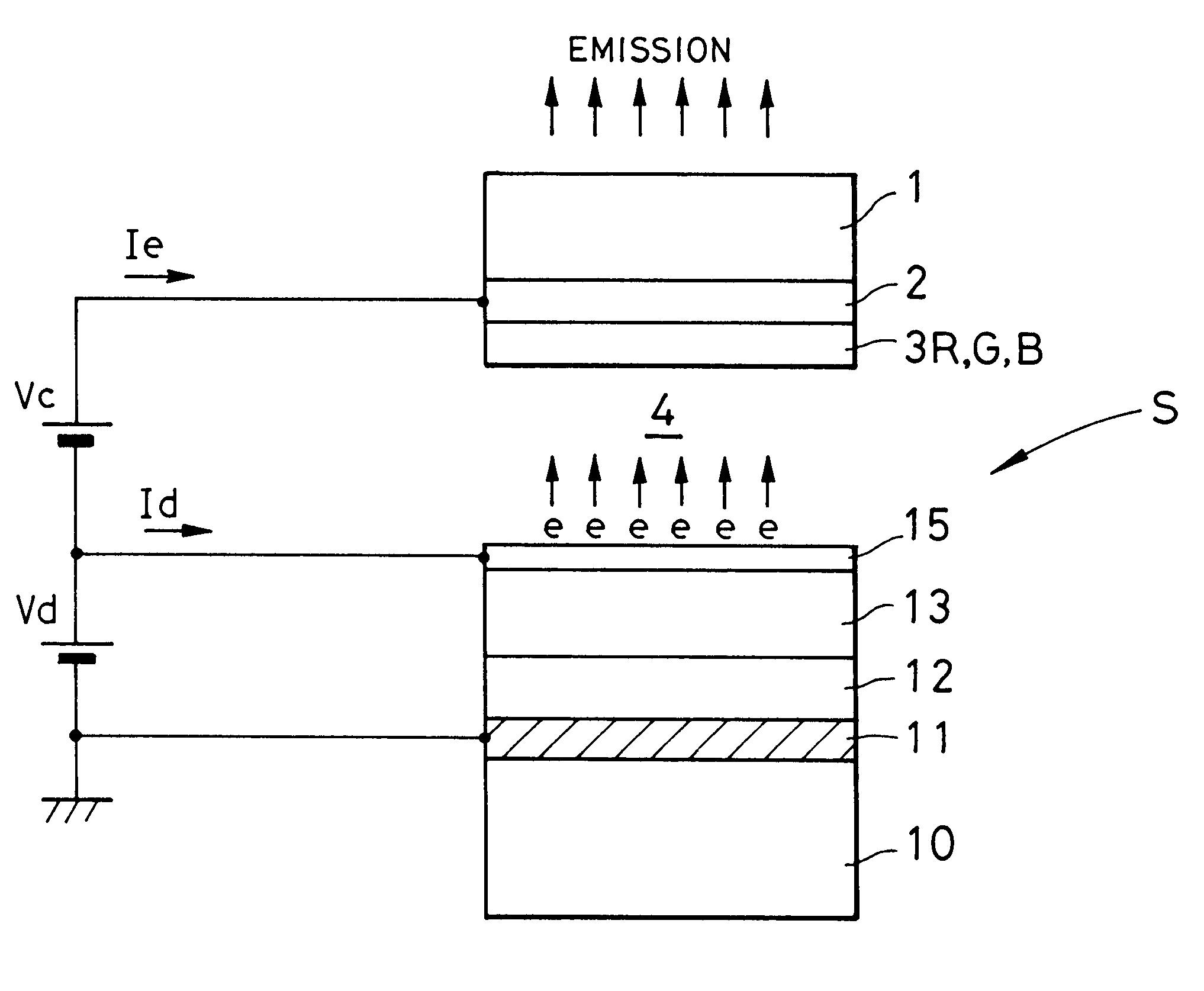
As illustrated in FIG. 1, one electron emission device "S" constructed in a stack configuration comprises; an ohmic electrode 11 made of aluminum (Al), tungsten (W), titanium nitride (TiN), copper (Cu), chromium (Cr) or the like on a first substrate 10 made of a glass or the like; an electron-supply layer 12 made of semiconductor such as silicon (Si) or the like on the ohmic electrode 11; an insulator layer 13 made of dielectric such as SiO.sub.x (X=0.1 to 2.0) or the like on the electron-supply layer 12; and a thin-film metal electrode 15 made of metal such as platinum (Pt), gold (Au) or the like facing a vacuum space on the insulator layer 13. Particularly, the insulator layer 13 is deposited in considerably thicker thicknesses so as to have a thickness of 50 nm or greater. Further, an additive material selected from atomic el...


PUM


Abstract

An electron emission device comprises an electron-supply layer made of metal or semiconductor and disposed on an ohmic electrode; an insulator layer formed on the electron-supply layer; and a thin-film metal electrode formed on the insulator layer. The electron-supply layer is essentially composed of elements belonging to group IV and contains an additive of at least one material selected from atomic elements belonging to group III or V.

Description

1. Field of the InventionThe present invention relates generally to an electron emission device, and more particularly to an electron emission display device which has a plurality of electron emission devices arranged in an image display array, for example, in a matrix form.2. Description of the Related ArtConventionally, in field electron emission display apparatuses, a Field Emission Display (FED) is known as a planar emission display device equipped with an array of cold cathode electron emission sources which does not require cathode heating. The emission principle of, for example, an FED using Spindt-type cold cathodes of minute protrusions is as follows. Its emission principle is like a Cathode Ray Tube (CRT), although this FED has a cathode array of Spindt-type protrusions which is different from that of CRT. In the FED, electrons are drawn into a vacuum space by means of each gate electrode spaced apart from the Spindt-type cathode, and the electrons are made to impinge upon...

Claims


Application Information

Patent Timeline
IPC IPC(8): H01J1/30H01J1/312H01J29/04H01J31/12
CPCH01J1/312B82Y10/00
Inventor NEGISHI, NOBUYASUHATA, TAKUYAYOSHIZAWA, ATSUSHISATOH, HIDEOYAMADA, TAKASHICHUMAN, TAKASHIIWASAKI, SHINGOYOSHIKAWA, TAKAMASAITO, HIROSHIOGASAWARA, KIYOHIDE
Owner PIONEER CORP
Why Eureka
Try Eureka