Multi-layer hard mask for deep trench silicon etch

a silicon substrate and deep trench technology, applied in the field of semiconductor manufacturing, can solve the problems of increasing manufacturing costs, affecting the control and precision of silicon substrate manufacturing, and many problems in deep trench etching of silicon substrates, so as to minimize the moisture sensitivity of the layer of bsg and enhance chemical vapor deposition

Inactive Publication Date: 2002-08-27
IBM CORP
View PDF21 Cites 31 Cited by
  • Summary
  • Abstract
  • Description
  • Claims
  • Application Information

AI Technical Summary

Benefits of technology

In still yet another aspect, the present invention relates to an intermediate silicon substrate for use in deep trench etching comprising: a silicon substrate; a layer of pad dielectric disposed on the silicon substrate; a layer of BSG disposed on the layer of pad dielectric; a layer of silicon oxide disposed on the layer of BSG by plasma enhanced chemical vapor d...

Problems solved by technology

Deep trench etching of the silicon substrate has many problems during the etching process and in the post-etch processing of the substrate.
However, the manufacturing sensitivity of the silicon substrate can inhibit control and precision during the etching process.
In addition, manufacturing costs are driven up when there are multiple masking s...

Method used


Image

  • Multi-layer hard mask for deep trench silicon etch
  • Multi-layer hard mask for deep trench silicon etch
  • Multi-layer hard mask for deep trench silicon etch

Examples


Embodiment Construction

)

In describing the preferred embodiments of the present invention, reference will be made herein to FIGS. 1-18 of the drawings in which like numerals refer to like features of the invention. Features of the invention are not necessarily shown to scale in the drawings.

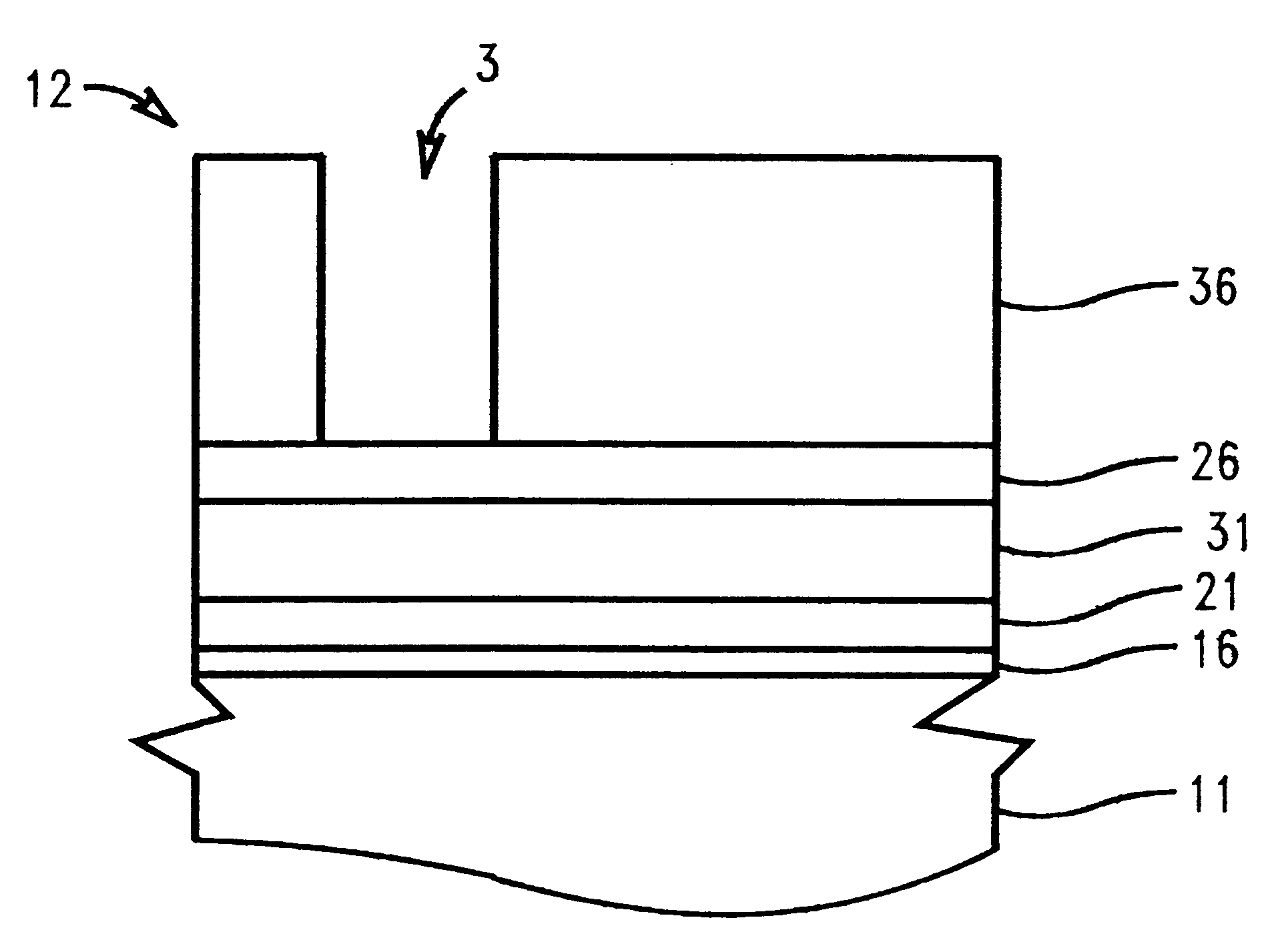
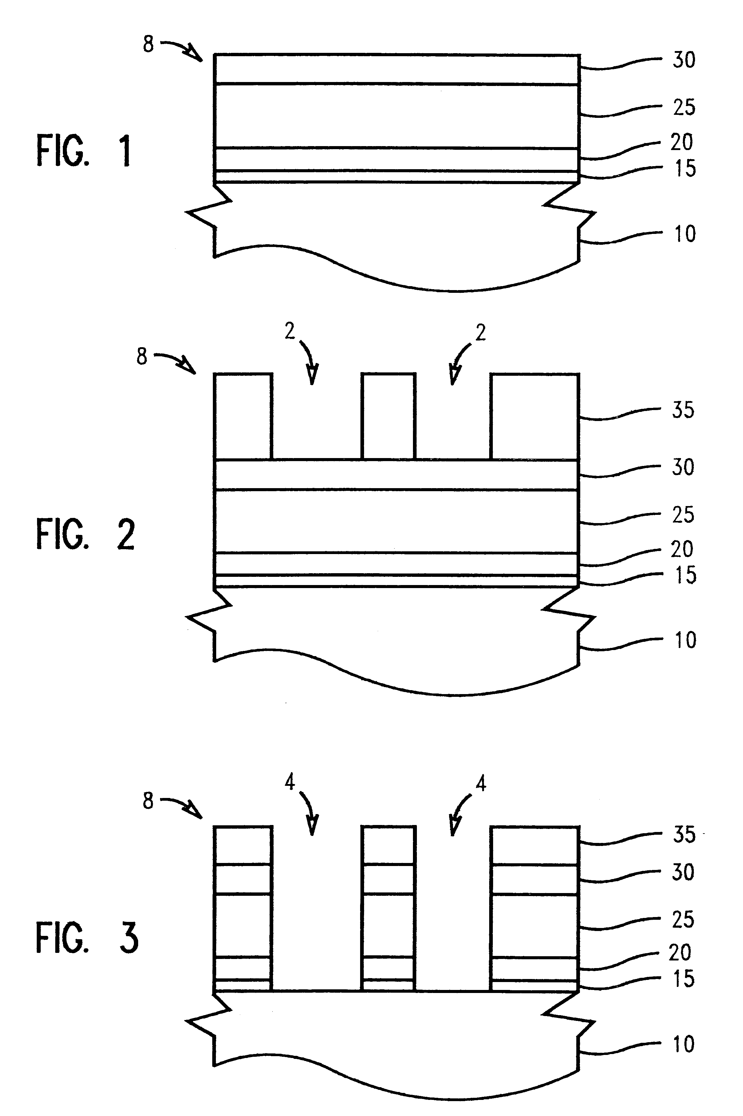
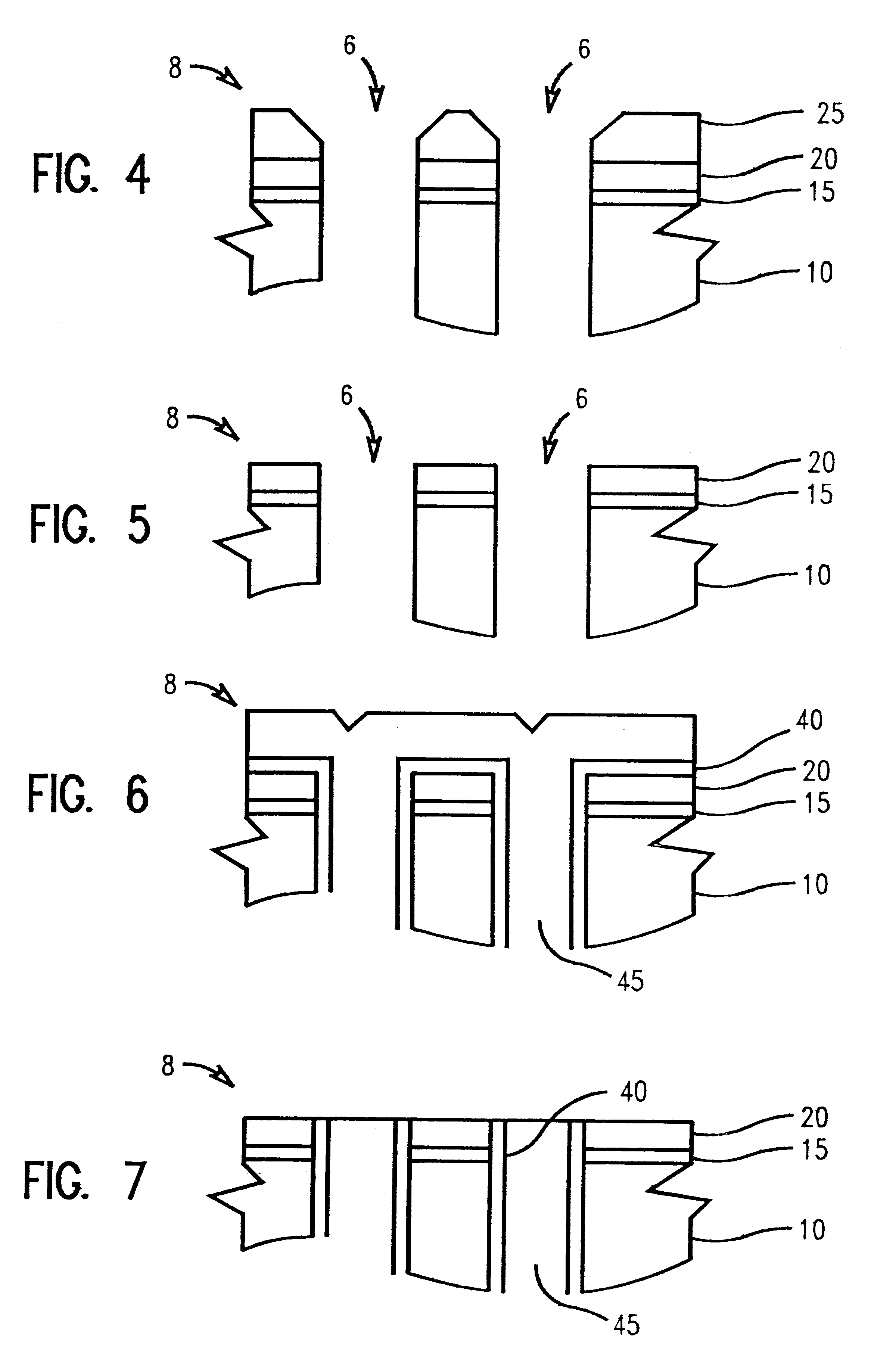
FIGS. 1-7 show a specific preferred embodiment of the method of deep trench silicon etching wherein the trenches are of close proximity. In FIG. 1, a method of etching trenches of close proximity on a semiconductor substrate comprises the steps of depositing a pad dielectric layer and a hard mask layer on silicon substrate 10 to form layered intermediate substrate 8. The pad dielectric layer comprises a first layer 15, preferably, silicon oxide, deposited on the substrate 10 followed by a second layer 20, preferably, silicon nitride, deposited over the first layer 15. A dual layer hard mask is then formed over the pad dielectric layer. The lower layer in the hard mask, or first layer, comprises a material 25 that etches...


PUM


Abstract

A method of etching multiple films with a dual layer hard mask wherein one layer is totally removed and the other layer partially removed during deep trench etching of the silicon substrate. In particular, a method of deep trench etching silicon substrates comprising the steps of providing a semiconductor substrate capable of being etched, with HBr/NF3/He/O2, having a layer of pad dielectric disposed depositing a layer of material capable of selective removability with respect to the pad dielectric, preferably BSG; depositing a layer of material having a slower etch rate than the semiconductor substrate and the layer of material capable of selective removability with respect to the pad dielectric, preferably, silicon oxide deposited by PECVD; patterning at least one of the layers, and etching the semiconductor substrate to form a trench and removing the layer of material having a slower etch rate than the semiconductor substrate, wherein trenches are of close proximity to each other.

Description

1. Field of the InventionThis invention relates to the field of semiconductor manufacture, and more specifically to the formation of deep trenches when etching silicon.This invention describes a process for etching multiple films with a dual layer hard mask, and specifically a process for etching deep trenches for DRAMs having a dual layer hard mask. The top hard mask is totally and the lower hard mask is partially removed while etching the deep trench.2. Description of Related ArtIn the formation of integrated circuits, it is often necessary to etch a trench in the silicon substrate. In particular, the trend towards packing more memory cells into a given chip area has led to the development of trench memory cells which require deep, narrow apertures in the silicon substrate. Trench memory cells and trench capacitors with one or more polysilicon electrodes for silicon integrated circuits have applications in structures known as dynamic random access memories (DRAMs).Deep trench etch...

Claims


Application Information

Patent Timeline
IPC IPC(8): H01L21/02H01L21/302H01L21/3065H01L21/308H01L21/311H01L21/8242
CPCH01L21/3065H01L21/3081H01L21/3085H01L21/31111H01L27/1087H10B12/0387
Inventor CANALE, ANTHONY J.CRONIN, JOHN E.
Owner IBM CORP
Why Eureka
Try Eureka