Low power voltage regulator with improved on-chip noise isolation

Inactive Publication Date: 2002-08-27
NXP USA INC
View PDF5 Cites 61 Cited by
  • Summary
  • Abstract
  • Description
  • Claims
  • Application Information

AI Technical Summary

Problems solved by technology

Variations between no load and full load current, such as may occur with digital circuits, can cause large switching noise that must be filtered to prevent errors in CMOS analog circuits on the same integrated circuit substrate or chip.
That unused portion of the full load current in excess of the load current is shunted through a shunt device in the shunt regulator and so, wasted.
High frequency circuits, and especially radio frequency (RF) circuits, are very sensitive to noise.
Switching noise from digital circuits can easily couple into radio frequency circuits thereby, degrading circuit performance.
Further, as digital circuit performance improves, digital functions are also being combined with RF functions onto monolithic integrated circuit chips integrating more and more digital and RF circuits onto the same chip and resulting in an increased number of local potential noise sources on a given chip.
Accordingly, when the load is less than full, Noro wastes some of the power supplied.
Unfortunately, the Curtis shunt regulator also consume & excess power when it is not fully loaded.
Unfortunately, these typical prior art shunt regulators suffer from excessive power consumption, while only providing limited isolation between digital and RF circuits that are integrated onto the same integrated circuit chip.

Method used


Image

  • Low power voltage regulator with improved on-chip noise isolation
  • Low power voltage regulator with improved on-chip noise isolation
  • Low power voltage regulator with improved on-chip noise isolation

Examples


Embodiment Construction

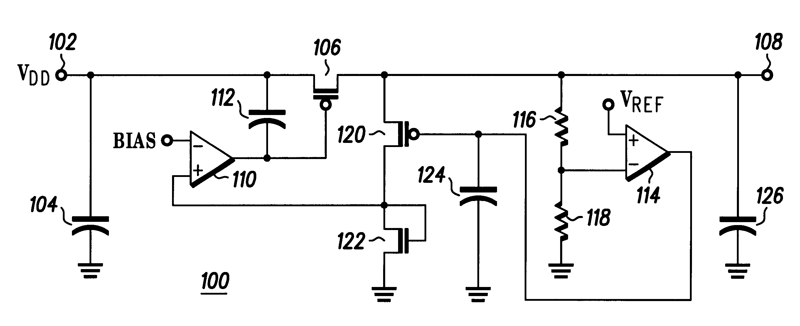
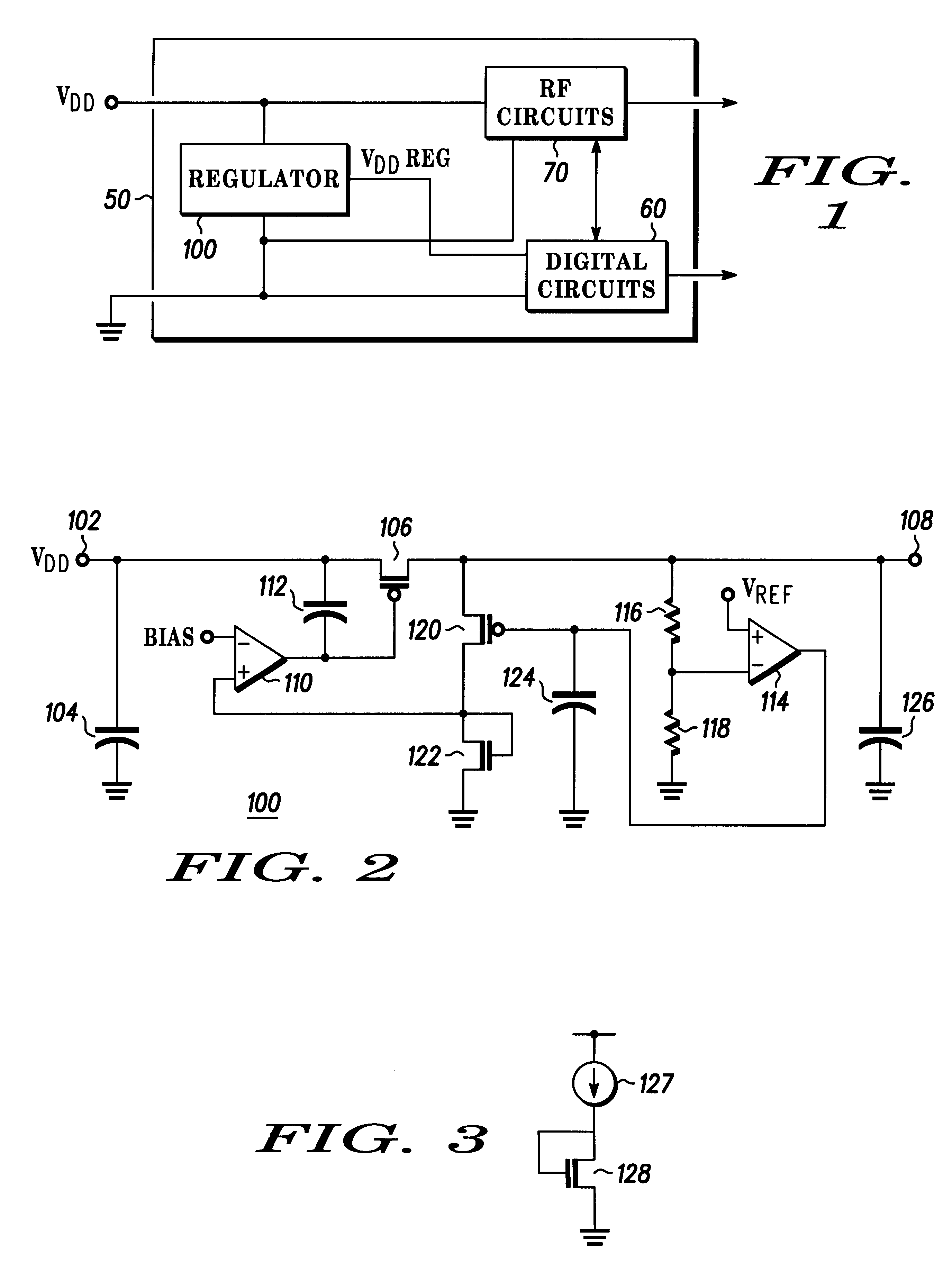
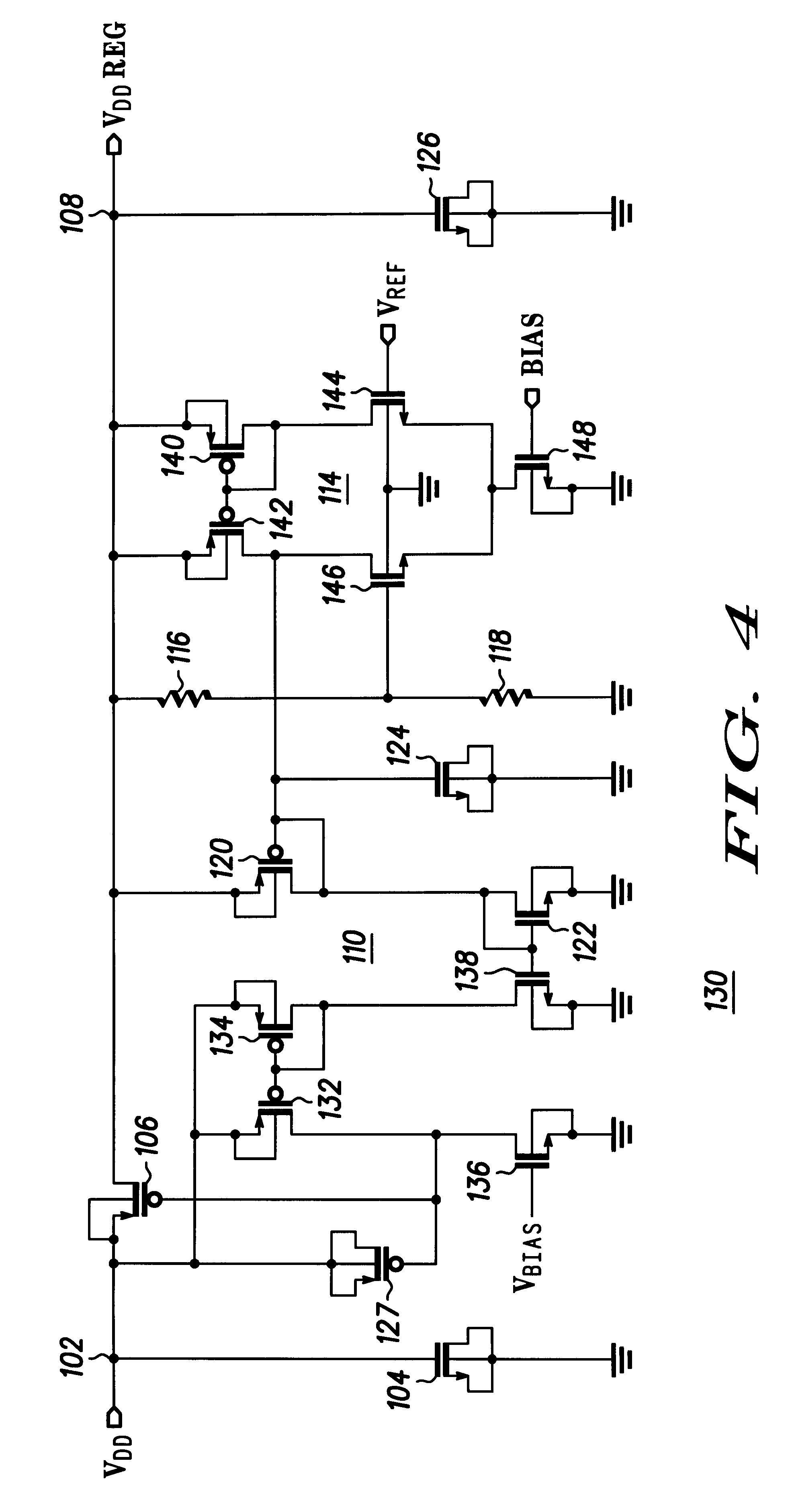
The present invention is a voltage regulator, which may be termed a shunt regulator, for isolating radio frequency circuits from on-chip digital circuit originated noise and the integrated circuit chip. Unlike prior art shunt regulators, which constantly supply full current, shunting any current not used by the load; the voltage regulator of the present invention constantly shunts a minimum current, e.g., 1 mA, and supplies whatever current needed for the load in excess of that minimum, responsive to variations in the shunt current. The voltage regulator includes regulator device (a PFET) driven by a sense amplifier to derive a regulator voltage from a supply voltage. Another sense amplifier senses changes in output voltage resulting from load current changes and adjusts current through a current shunt so that the current shunt shunts excess load current. The sense amplifier driving the regulator device senses current flow through the current shunt and adjusts the current supplied b...


PUM


Abstract

A voltage regulator 100, 130 for isolating radio frequency circuits from on chip digital circuit originated noise and an integrated circuit chip including the voltage regulator. The voltage regulator 100, 130 includes regulator device (a PFET) 106 driven by a sense amplifier 110 to derive a regulator voltage 108 from a supply voltage 102. Another sense amplifier 114 senses changes in output load and adjusts current flow through a current shunt 120, 122 so that the current shunt 120, 122 shunts excess load current. The sense amplifier 110 driving the voltage regulator device 106 senses current flow through the current shunt 120, 122 and adjusts the current supplied by the regulator device 106 to reduce excess current. The current shunt 120, 122 is a series connected PFET 120 and NFET diode 122, with the gate of the PFET 120 driven to control current flow. Each of the sense amplifiers 110, 114 includes a pair of PFETs 132, 134 140, 142 and a pair of NFETs 136, 138 144, 146, the drain of each PFET of the pair is tied to a corresponding drain of one of the pair of NFETs. A voltage divider 116, 118 connected between the regulator voltage 108 and ground provides a sense voltage to the output sense amplifier 114 so that the output sense amplifier compares the sense voltage against a reference voltage (VREF) to determine whether the regulator device is providing too much, not enough or just the right output current level.

Description

1. Field of the InventionThe present invention is related to power supply regulators for radio frequency applications and more particularly to a shunt regulator for high frequency applications.2. Background DescriptionVoltage regulators are well known. An ideal voltage regulator provides a constant voltage regardless of load. Thus, the voltage regulator provides the same voltage under no load (at no current) as it does fully loaded. Current used by circuits in the complementary insulated gate field effect transistor (FET) technology, commonly known as CMOS, primarily, is switching current with negligible static (or DC) current flow.CMOS circuit current flow usually occurs only during switching, primarily, either to charge or discharge the circuit's load (capacitance). Thus, digital circuits that are synchronized by a common clock signal may exhibit sporadic episodes of very high switching current, e.g., from a counter switching from FFFF.sub.16 to OOOO.sub.16. By contrast, typical r...

Claims


Application Information

Patent Timeline
IPC IPC(8): G05F1/10G05F1/575
CPCG05F1/575
Inventor CONNELL, LAWRENCE EDWINMCCARTHY, DANIEL PATRICK
Owner NXP USA INC
Why Eureka
Try Eureka