Frequency-doubling delay locked loop

a delay lock and frequency technology, applied in the field of frequency double delay lock loop, can solve the problems of analog plls suffering from a number of general drawbacks, general unsuitability of pll-based clock generation systems, and inability to meet the requirements of plls

Inactive Publication Date: 2002-08-27
CONVERSANT INTPROP MANAGEMENT INC
View PDF11 Cites 89 Cited by
  • Summary
  • Abstract
  • Description
  • Claims
  • Application Information

AI Technical Summary

Problems solved by technology

However, PLL-based clock generation systems are generally unsuitable if the interface clock is intermittent (i.e. not continuous) and if it is necessary to restore the desired phase and frequency relationship between the interface clock and internal clock quickly when the interface clock reappears.
In addition, PLLs are also unsuitable if it is necessary for the internal clock to accurately track high frequency phase jitter in the interface reference clock.
More generally, analog PLLs suffer from a number of general drawbacks in today's mainly digital memory design environment.
Firstly, PLLs employ analog elements which typically consume substantially more power than digital elements due to their de bias current requirements.
Secondly, recent trends towards decreasing power supply voltages for reducing power consu...

Method used


Image

  • Frequency-doubling delay locked loop
  • Frequency-doubling delay locked loop
  • Frequency-doubling delay locked loop

Examples


first embodiment

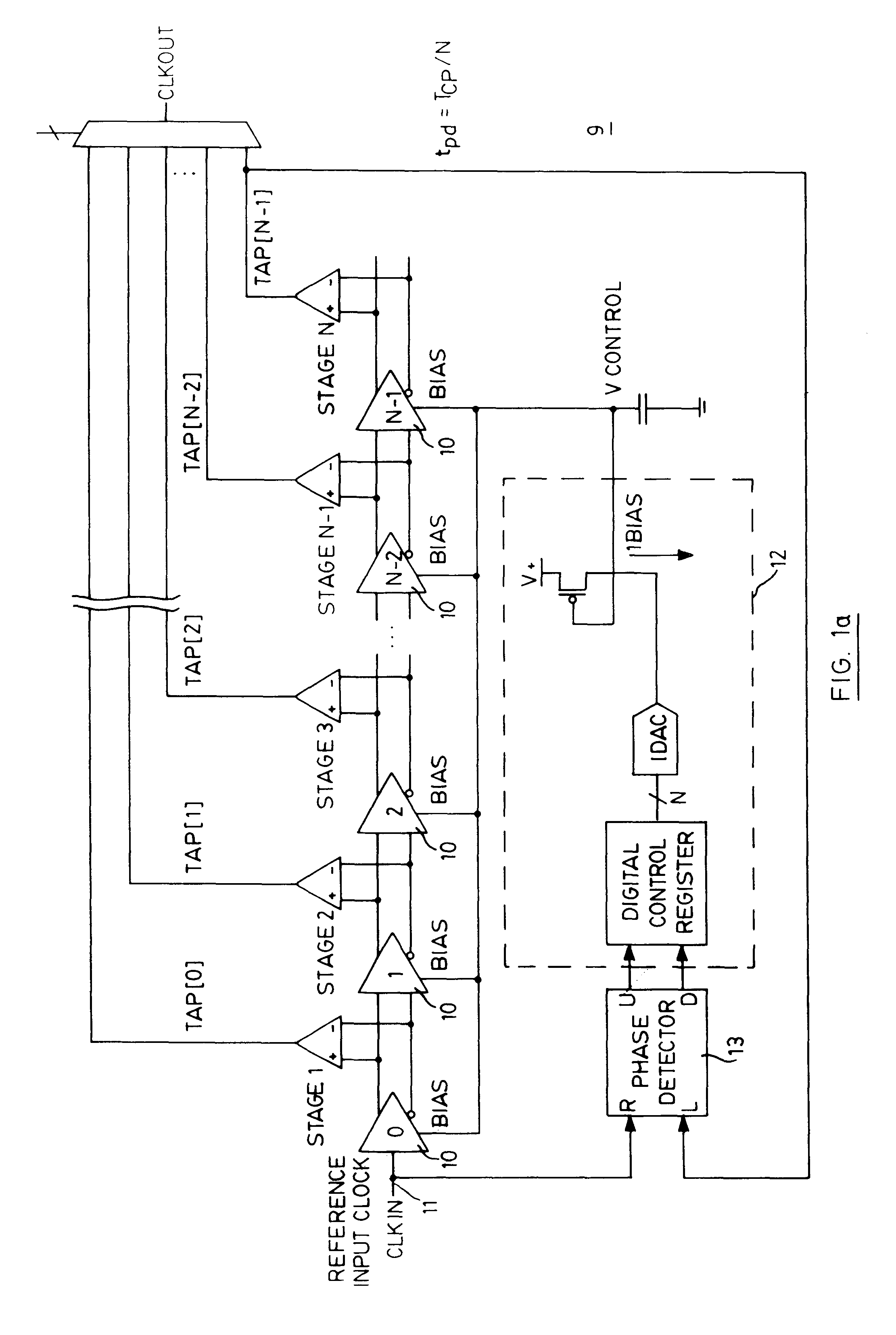
FIG. 4(a) illustrates an alternate embodiment of the frequency doubling DLL invention employing duty cycle colon. Similarly to the first embodiment discussed with reference to FIG. 3(a), an N-stage period-matched DLL (with N being divisible by 4) is used to provide (N-1) outputs TAP[N-1], where each delay stage 30 provides one TAP[i] output. In this alternate embodiment however, the N / 4-1 TOG cells have 4 inputs per cell instead of just 2. Specifically, the outputs of all N delay stages are connected to N / 4 TOG cells. The 0 degree, 90 degree 180 degree, and 270 degree inputs to each TOG cell are connected to the output of delay elements consecutively separated by N / 4 stages. For example, TOG cell 0 receives TAP[0] at its 0 degree input, TAP [N / 4 ] at its 90 degree input, TAP[2N / 4] at its 180 degree input and TAP[3N / 4] at its 270 degree input. Together, all the true (T) and complimentary (C) outputs of the N / 4 TOG cells 31, 32, . . . 33 PHI[0]) . . . PHI[N / 2-1] present N / 2 distinct p...

second embodiment

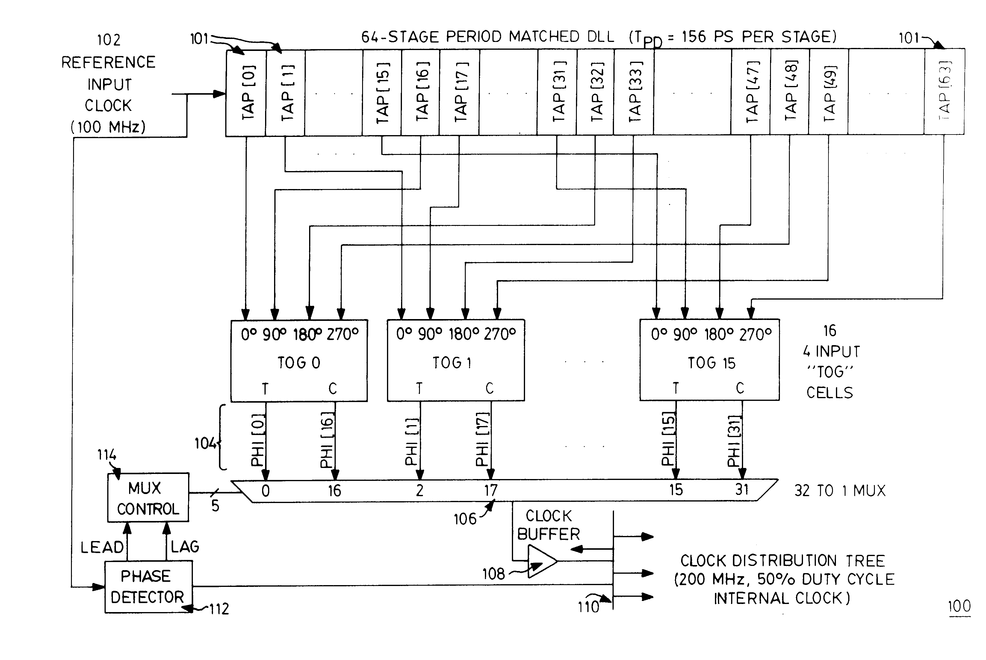
For applications where the phase relationship between the reference input clock and the frequency doubled internal clock is important, the N / 2 output clock phases from the frequency doubling DLL can be fed to the inputs of a N / 2 to 1 multiplexer. By adding a phase detector and MUX control logic, it is possible to chose the most appropriate clock phase from the N / 2 clock phase outputs. A full clock generating scheme comprising the frequency doubling DLL with duty cycle correction invention for use in a memory interface ASIC is represented generally in FIG. 6 by the numeral 100 or delay elements 101. In this implementation, N=64 stages and the input reference clock 102 is nominally 100 MHz (Tcp=10.0 ns). It can be seen that the resolution depends on the number of delay elements 101. The DLL generates 32 phases 104 of a 50% duty cycle 200 MHz clock with each phase output spaced 720 / 64 or 11.25 degrees apart. A 32-input multiplexer 106 selects 1-of-32 phases to drive the clock buffer 10...


PUM


Abstract

A frequency multiplier circuit comprising a delay line receiving at one end thereof a reference clock for generating clock tap outputs from respective ones of a plurality of period matched delay elements; a clock combining circuit responsive to pairs of tap outputs for generating a rising and falling edge of an output clock pulse from respective ones of the pairs whereby the output clock period is less than the input clock period.

Description

This invention relates to the field of clock generation circuit for generating a high speed clock of a reference clock signal, and more particularly, to such circuits incorporating a delay locked loop (DLL).BACKGROUND TO THE INVENTIONIn many relatively self-contained electronic subsystems such as integrated circuits and multi-chip modules, an internal clock is used to synchronize operations. Often the frequency of the internal clock is higher than the frequency of an external interface clock which is used to synchronize the transfer data and control information to and from the subsystem. It is often necessary to establish a defined phase and frequency relationship between the internal clock and the slower external interface clock for efficient low latency operation of the interface. As an example, a common requirement is to have the internal clock signal be exactly twice the frequency of the interface clock. Even tighter restrictions might require that rising edges of the inter cloc...

Claims


Application Information

Patent Timeline
IPC IPC(8): H03K5/15H03L7/08H03L7/07H03L7/081H03K5/00H03L7/16G11C11/407G06F1/08H03K5/133
CPCH03K5/00006H03K5/15046H03L7/07H03L7/0812H03L7/0814H03L7/16H03L7/06H03L7/089H03L7/0816H03L7/00
Inventor DEMONE, PAUL W.
Owner CONVERSANT INTPROP MANAGEMENT INC
Why Eureka
Try Eureka