Substrate structures for integrated series connected photovoltaic arrays and process of manufacture of such arrays

a photovoltaic array and integrated series technology, applied in photovoltaics, electrical devices, semiconductor devices, etc., can solve the problems of high cost of single crystal silicon material and interconnection processing, thwarting wide-scale energy collection using single-crystal silicon cells, and reducing the efficiency of photovoltaic energy collection, etc., to achieve low cost, low cost, and high efficiency.

a photovoltaic array and integrated series technology, applied in photovoltaics, electrical devices, semiconductor devices, etc., can solve the problems of high cost of single crystal silicon material and interconnection processing, thwarting wide-scale energy collection using single-crystal silicon cells, and reducing the efficiency of photovoltaic energy collection, etc., to achieve low cost, low cost, and high efficiency.

US6459032B1Inactive Publication Date: 2002-10-01SOLANNEX

Image

  • Substrate structures for integrated series connected photovoltaic arrays and process of manufacture of such arrays
  • Substrate structures for integrated series connected photovoltaic arrays and process of manufacture of such arrays
  • Substrate structures for integrated series connected photovoltaic arrays and process of manufacture of such arrays

Examples


Embodiment Construction

Reference will now be made in detail to the preferred embodiments of the invention, examples of which are illustrated in the accompanying drawings. In the drawings, like reference numerals designate identical or corresponding parts throughout several views and an additional letter designation is characteristic of a particular embodiment.

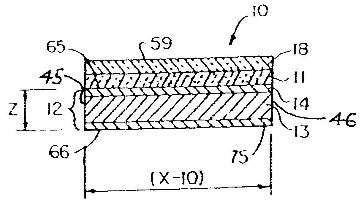
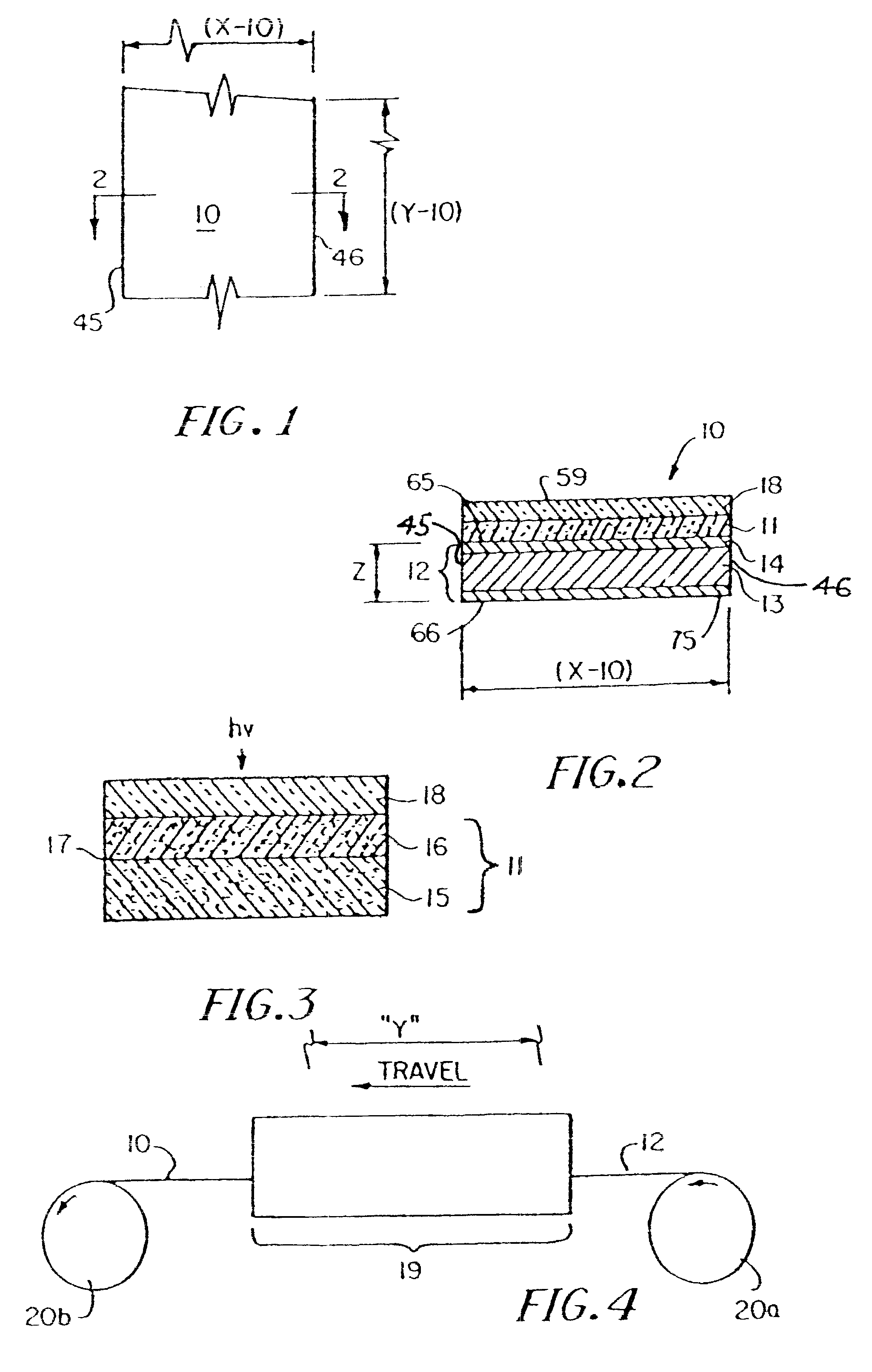
Referring to FIGS. 1 and 2, a thin film photovoltaic cell, including a supporting conductive foil is generally indicated by 10. Cell 10 has a top surface 59 and comprises a thin film photovoltaic structure 11 supported by conductive foil 12.

Foil 12 has a width X-10, length Y-10 and thickness Z-10. The full extent of width X-10 of foil 12 defines a first photovoltaic cell terminal edge 45 and second photovoltaic cell terminal edge 46. It is contemplated that length Y-10 is considerably greater than width X-10 and length Y-10 can generally be described as "continuous" or being able to be processed in a roll-to-roll fashion. Foil 12 has first surface 65...


PUM


Abstract

This invention comprises deposition of thin film photovoltaic junctions on conductive foil substrates which can be heat treated following deposition in a continuous fashion without deterioration of the metal support structure. In a separate operation, an interconnection substrate structure is produced in a continuous roll-to-roll fashion. The conductive foil supported photovoltaic junction is then laminated to the interconnection substrate structure and conductive connections are deposited to complete the module or array. In this way the interconnection substrate structure can be uniquely formulated from polymer-based materials since it does not have to endure high temperature exposure. Furthermore, the photovoltaic junction and its conductive foil support can be produced in bulk without the need to use the expensive and intricate material removal operations currently taught in the art to achieve series interconnections.

Description

Photovoltaic cells have developed according to two distinct methods. The initial operational cells employed a matrix of single crystal silicon appropriately doped to produce a planar p-n junction. An intrinsic electric field established at the p-n junction produces a voltage by directing solar photon produced holes and free electrons in opposite directions. Despite good conversion efficiencies and long-term reliability, widespread energy collection using single-crystal silicon cells is thwarted by the exceptionally high cost of single crystal silicon material and interconnection processing.A second approach to produce photovoltaic cells is by depositing thin photovoltaic semiconductor films on a supporting substrate. These thin semiconductor films are normally less than 30 micrometers thick and typically 0.05 to 5 micrometers thick. Material requirements are minimized and technologies can be proposed for mass production. The thin film structures can be designed according to doped ho...

Claims


Application Information

Patent Timeline
01 Oct 2002
Publication
US6459032B1
IPC
H01L31/0392; H01L31/036; H01L31/05
CPC
H01L31/0392; H01L31/0512; H01L31/0508; Y02E10/50; H01L31/0504; H01L31/0445
Inventors
LUCH, DANIEL