Chemically synthesized and assembled electronics devices

a technology of electronics and electronics, applied in the field of chemically synthesized and assembled electronics devices, can solve the problems of affecting the rate of charge transport across the wire junction, and achieve the effect of simple and inexpensive implementation

Inactive Publication Date: 2002-10-01
HEWLETT PACKARD CO +1
View PDF9 Cites 266 Cited by
  • Summary
  • Abstract
  • Description
  • Claims
  • Application Information

AI Technical Summary

Benefits of technology

In accordance with the present invention, a route to the fabrication of electronic devices is provided, in which the devices consist of two crossed wires sandwiching an electrically addressable molecular species. The approach is extremely simple and inexpensive to implement, and scales from wire dimensions of several micrometers down to nanometer-scale dimensions. The device of the present invention can be used to produce crossbar switch arrays, logic devices, memory devices, and communication and signal routing devices.
The present invention enables construction of molecular electronic devices on a length scale than can range from micrometers to nanometers via a straightforward and inexpensive chemical assembly procedure. The device is either partially or completely chemically assembled, and the key to the scaling is that the location of the devices on the substrate are defined once the devices have been assembled, not prior to assembly.
The present invention solves several problems that currently plague current solid state electronic device technology. First, the fundamental device unit is a molecule or a layer of molecules at the junction of two wires, and so the devices will scale down from wires of micrometer length scales to wires of molecular length scales (a nanometer, for example) without appreciable change in device operation. Second, molecular devices are voltage, not electric field, addressable. This means that molecular switches can be set at one voltage, and the state of the switch can be read at another voltage (either smaller in magnitude or a different polarity), and only two wires are required for the entire process. In most solid-state devices, a total of four wires are required to set and subsequently read the state of a switch. These include two wires that are required to set the state of a switch, and two different wires that are required to read the state of that switch. Third, the devices that are fabricated are extremely versatile, and can be configured to carry out any number of tasks, ranging from memory to logic to communication and signal routing to energy storage. Finally, since only two wires are needed to address and read these devices, and since the device itself is defined not by high resolution lithographic templating, but rather by the relatively arbitrary intersection of two wires, the fabrication process for these wires is substantially simpler and more tolerant of manufacturing deficiencies than is the current art.

Problems solved by technology

Oxidation or reduction will affect the tunneling distance or the tunneling barrier height between the two wires, thereby exponentially altering the rate of charge transport across the wire junction.
Second, molecular devices are voltage, not electric field, addressable.

Method used


Image

  • Chemically synthesized and assembled electronics devices
  • Chemically synthesized and assembled electronics devices
  • Chemically synthesized and assembled electronics devices

Examples


examples

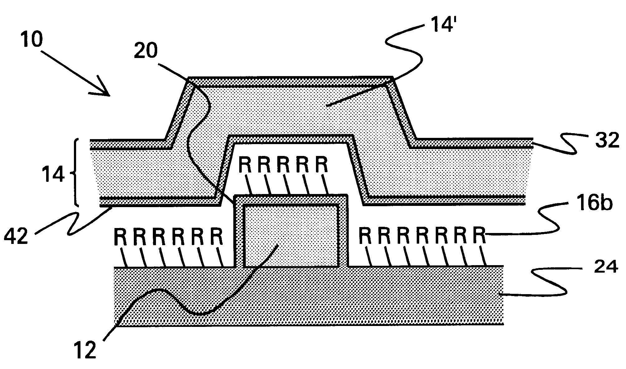
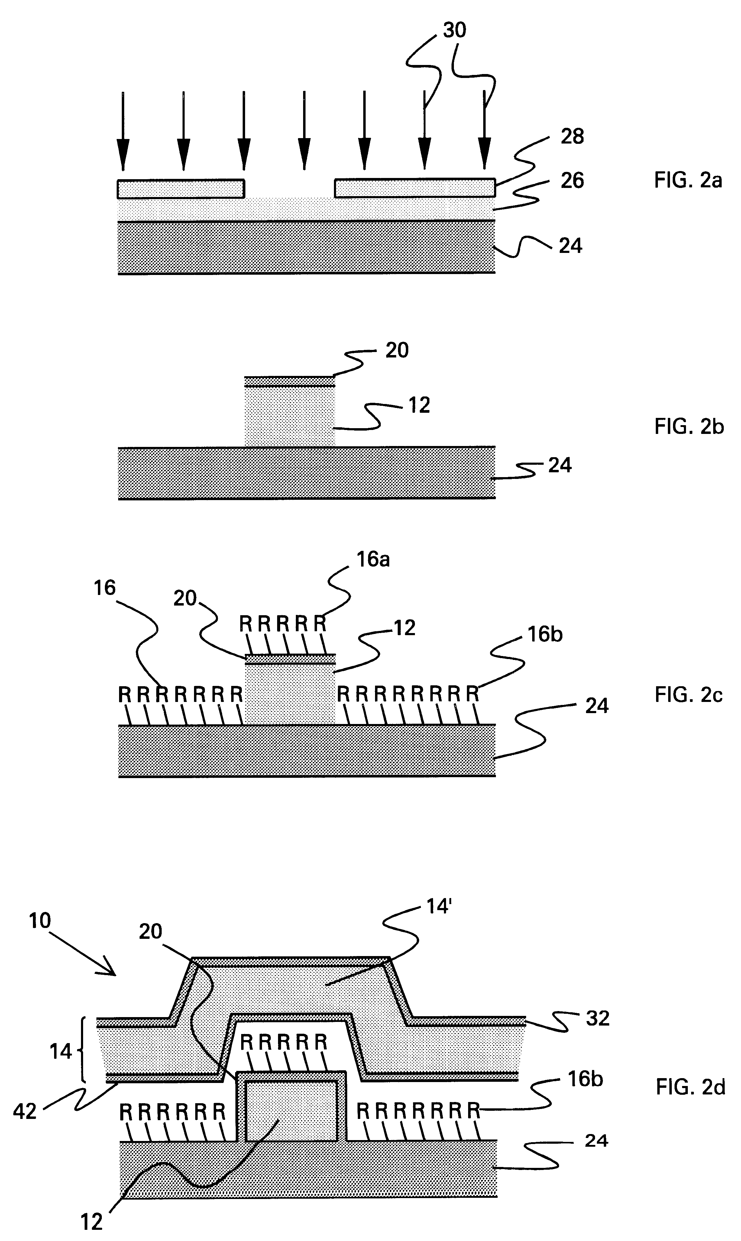
The present invention was reduced to practice to make a molecular switch-based device that could be configured as an electrically configurable read-only-memory, nonlinear logic gates that operated as diode-based logic, or a signal routing device. The device was made according to the method described in FIGS. 2A-2D, with the following modifications: A 5 micrometer wide aluminum wire 12 was deposited on a silica substrate 24 using conventional lithographic procedures. The wire 12 was provided with an oxide coating 14 of Al.sub.2 O.sub.3, which naturally formed to a thickness of about 1.0 to 1.5 nm when the aluminum wire was exposed to air. One of the molecular species shown in FIGS. 4A-4C was dissolved in tetrahydrofuran solvent, prepared as a Langmuir monolayer, and transferred as a Langmuir-Blodgett single molecular monolayer film 16 that covered the Al wire 12 and the silica substrate 24. The molecular compounds shown in FIGS. 4A-4C are from a class of molecular compounds known as ...


PUM

PropertyMeasurementUnit
sizeaaaaaaaaaa
heightsaaaaaaaaaa
diametersaaaaaaaaaa

Abstract

A route to the fabrication of electronic devices is provided, in which the devices consist of two crossed wires sandwiching an electrically addressable molecular species. The approach is extremely simple and inexpensive to implement, and scales from wire dimensions of several micrometers down to nanometer-scale dimensions. The device of the present invention can be used to produce crossbar switch arrays, logic devices, memory devices, and communication and signal routing devices. The present invention enables construction of molecular electronic devices on a length scale than can range from micrometers to nanometers via a straightforward and inexpensive chemical assembly procedure. The device is either partially or completely chemically assembled, and the key to the scaling is that the location of the devices on the substrate are defined once the devices have been assembled, not prior to assembly.

Description

The present invention relates generally to electronic devices whose functional length scales are measured in nanometers, and, more particularly, to simple devices used as building blocks to form more complicated structures, and to the methods for forming such devices. Devices both of micrometer and nanometer scale may be constructed in accordance with the teachings herein.The silicon (Si) integrated circuit (IC) has dominated electronics and has helped it grow to become one of the world's largest and most critical industries over the past thirty-five years. However, because of a combination of physical and economic reasons, the miniaturization that has accompanied the growth of Si ICs is reaching its limit. The present scale of devices is on the order of tenths of micrometers. New solutions are being proposed to take electronics to ever smaller levels; such current solutions are directed to constructing nanometer-scale devices.Prior proposed solutions to the problem of constructing ...

Claims


Application Information

Patent Timeline
Patent Type & Authority Patents(United States)
IPC IPC(8): B82B1/00G11C13/02H01L27/10B81B7/04G01R31/28H01L21/00H01L23/532H01L29/861H01L51/00H01L51/05H01L51/30H01L51/40
CPCB82B1/00B82Y10/00B82Y30/00G11C13/0009G11C13/0014G11C13/02H01L27/10H01L51/0595G11C2213/72G11C2213/77G11C2213/81Y10S977/936Y10S977/704Y10S977/705H10K10/701
Inventor HEATH, JAMES R.WILLIAMS, R. STANLEYKUEKES, PHILIP J.
Owner HEWLETT PACKARD CO
Why Eureka
Try Eureka