Design rule checking system and method

Inactive Publication Date: 2002-10-22
SYNOPSYS INC
View PDF53 Cites 526 Cited by
  • Summary
  • Abstract
  • Description
  • Claims
  • Application Information

AI Technical Summary

Benefits of technology

In some embodiments, the hierarchy in the corrected design is maintained throughout the process. This allows for a more efficient creation of the simulated image and the design rule checking process.
In other embodiments, a method of adding corrections to a design is described. In these embodiments, a simulated image is compared with the desired design. Design rule errors identified in the comparison can then be used to add corrections to the original design (e.g., by adding OPC type corrections). In some embodiments, the hierarchy of the design can be maintained, thereby increasing the efficiency of the system.
Other embodiments are capable of checking all advanced masks such as OPC, PSM, and their derivatives, at a single process layer, and enables inter-layer dependence checking on the global

Problems solved by technology

Besides the aforementioned design rules, the resolution value of the exposure tool used in optical lithography also places limits on the designers of integrated circuit layouts.
Flattening of the hierarchy typically results in several orders of magnitude increase in the size of data storage required to represent the pattern.
Currently, these operations require some sort of flattening of the original design data in order to be performed--resulting in an earlier than desired flattening of the design data.
Another problem that occurs when feature sizes and spacing approach the resolution limit of the lithographic tool is that corners (concave and convex) tend to overexpose

Method used


Image

  • Design rule checking system and method
  • Design rule checking system and method
  • Design rule checking system and method

Examples


Embodiment Construction

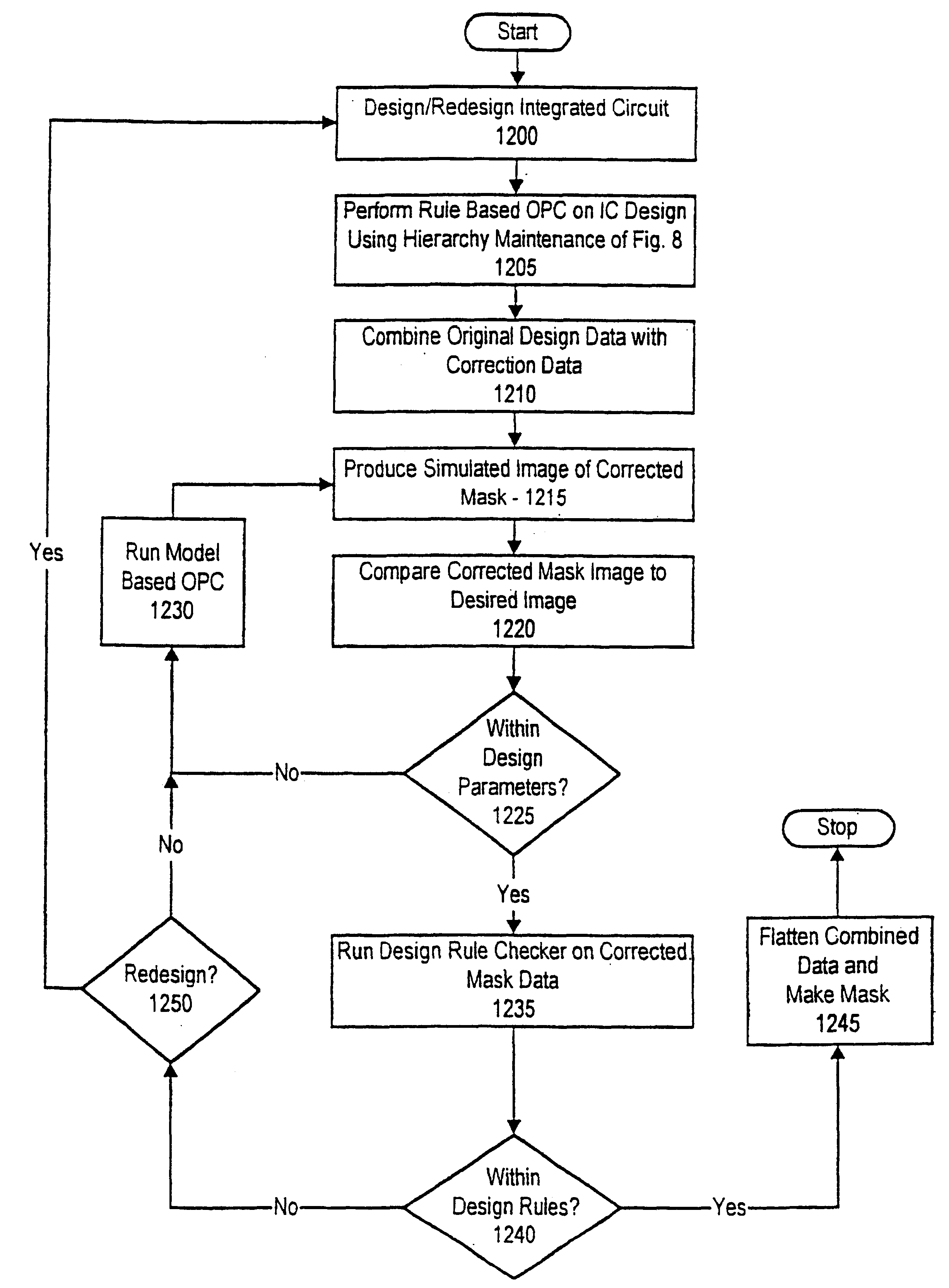
Before describing the details associated with design rule checking, a description of how the hierarchy in the designs is maintained is while different types of corrections and checking is performed. Then, a description of how simplified design rule checking is performed is described.

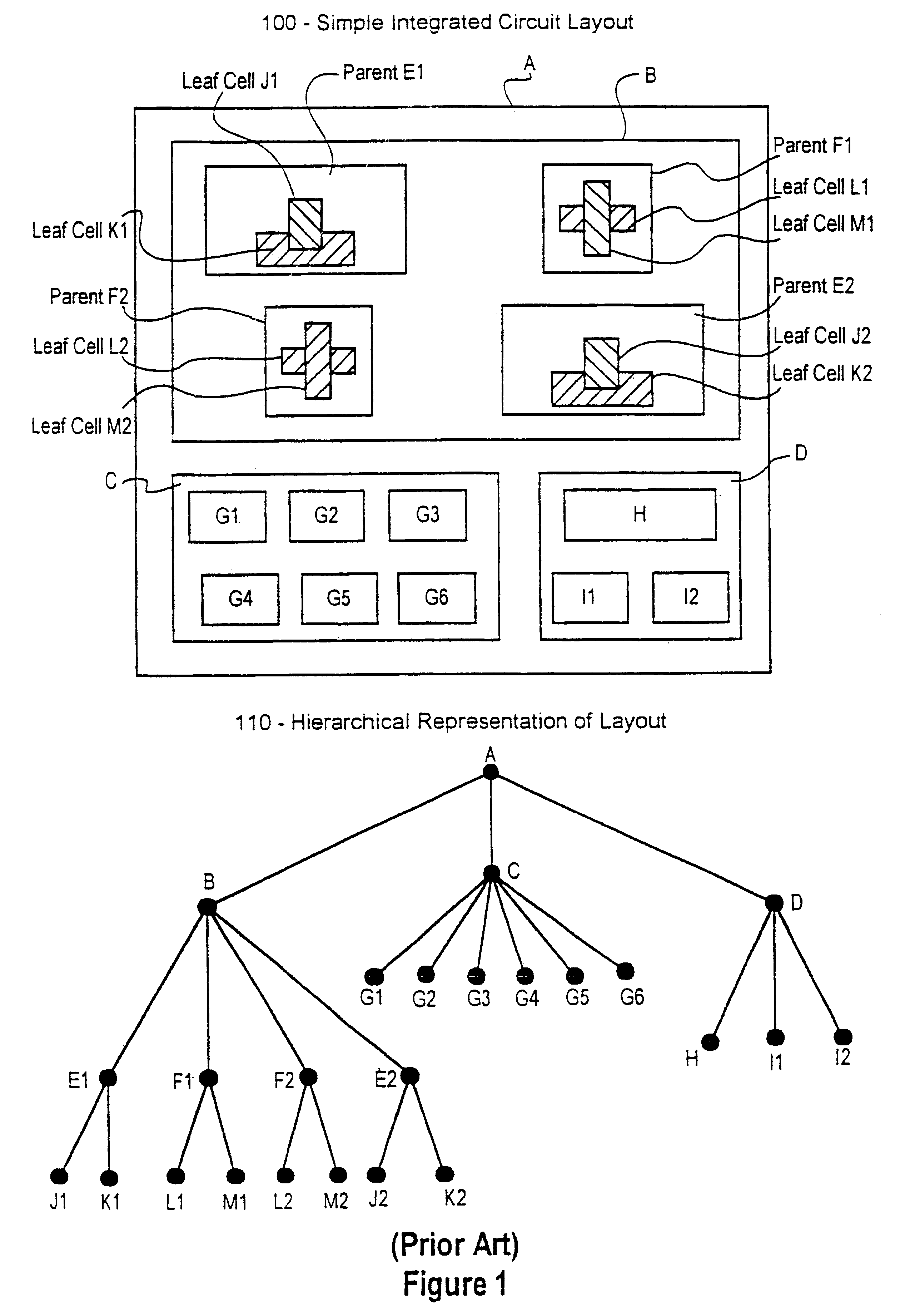
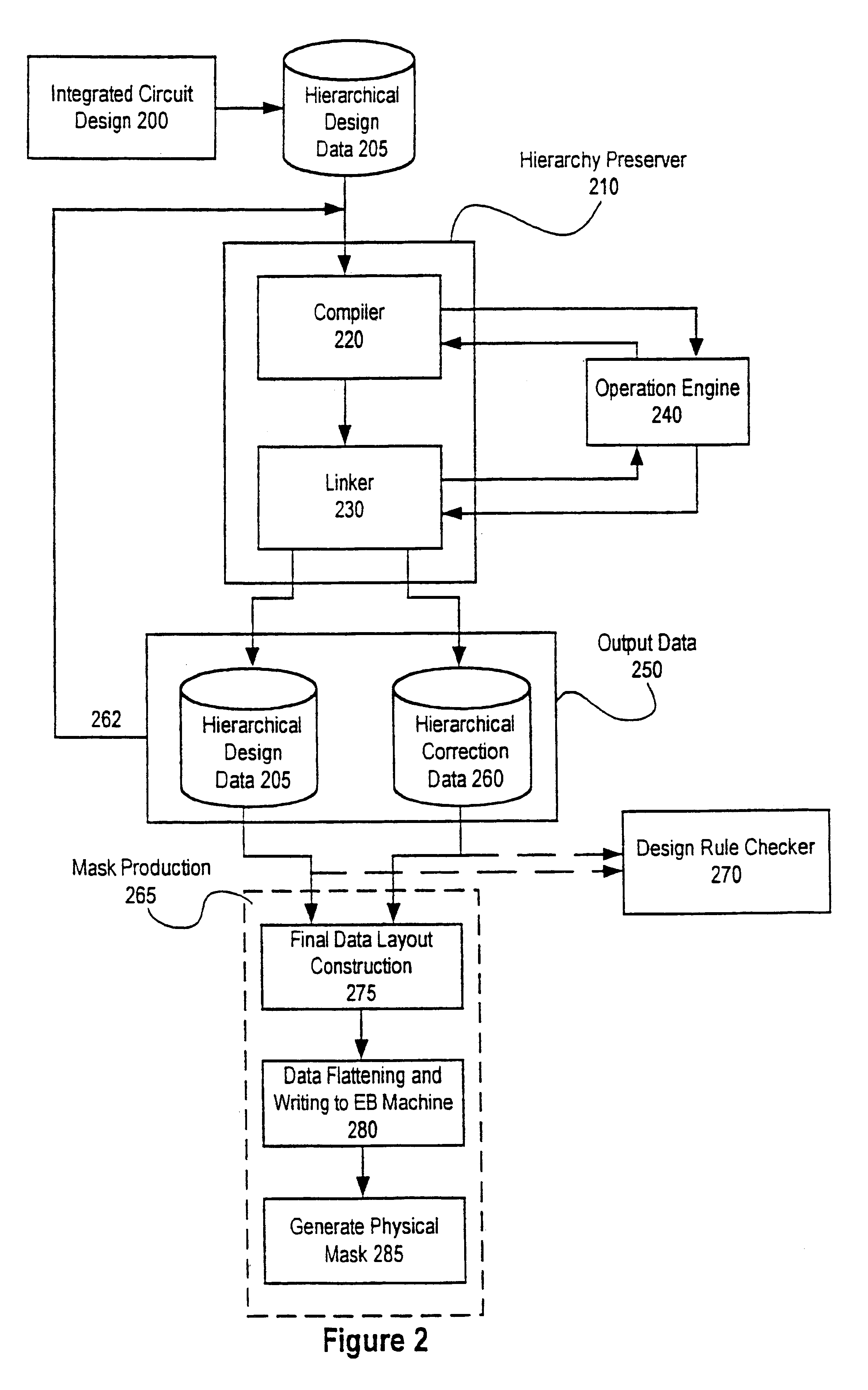
a. Maintenance of Hierarchy in Designs

As described above, in the manufacture of photolithography masks, it is advantageous to flatten the data representing the IC design at the latest point in the actual manufacture of the masks. However, this flattening takes place earlier than desired in some instances. This is because the original layout for a complicated IC is typically manipulated after the original design is completed in order to perform one of a number of operations on the design. These operations include the performance of logical operations, the generation of optical proximity corrections, the generation of phase shifting masks, and the design rule checking of masks that have undergone these ope...


PUM


Abstract

A method for performing design rule checking on OPC corrected or otherwise corrected designs is described. This method comprises accessing a corrected design and generating a simulated image. The simulated image corresponds to a simulation of an image which would be printed on a wafer if the wafer were exposed to an illumination source directed through the corrected design. The characteristics of the illumination source are determined by a set of lithography parameters. In creating the image, additional characteristics can be used to simulate portions of the fabrication process. However, what is important is that a resulting simulated image is created. The simulated image can then be used by the design rule checker. Importantly, the simulated image can be processed to reduce the number of vertices in the simulated image, relative to the number of vertices in the OPC corrected design layout. Also, the simulated image can be compared with an idea layout image, the results of which can then be used to reduce the amount of information that is needed to perform the design rule checking.

Description

THE BACKGROUND OF THE INVENTIONa. The Field of the InventionThis invention relates to the field of integrated circuit manufacturing. In particular, the invention relates to the concepts and implementation techniques to make fast and efficient integrated circuit layout design rule checking possible.b. Description of Related ArtIn designing an integrated circuit (IC), engineers typically rely upon computer simulation tools to help create a circuit schematic design consisting of individual devices coupled together to perform a certain function. To actually fabricate this circuit in a semiconductor substrate the circuit must be translated into a physical representation, or layout, which itself can then be transferred onto the silicon surface. Again, computer aided design (CAD) tools assist layout designers in the task of translating the discrete circuit elements into shapes which will embody the devices themselves in the completed IC. These shapes make up the individual components of th...

Claims


Application Information

Patent Timeline
IPC IPC(8): G03F9/00G06F17/50G03F1/00G03F1/36
CPCG03F1/144G03F1/36G06F17/5081G06F2217/12G06F30/398G06F2119/18
Inventor CHANG, FANG-CHENGWANG, YAO-TINGPATI, YAGYENSH C.
Owner SYNOPSYS INC
Why Eureka
Try Eureka