Method for manufacturing a ferroelectric capacitor having improved polarization characteristics and a method for manufacturing a ferroelectric memory device incorporating such capacitor
a technology of ferroelectric capacitors and polarization characteristics, which is applied in the direction of semiconductor devices, electrical devices, transistors, etc., can solve the problems of affecting the development of practical devices, and affecting the reliability of repeat reading or writing operations,
- Summary
- Abstract
- Description
- Claims
- Application Information
AI Technical Summary
Benefits of technology
Problems solved by technology
Method used
Image
Examples
embodiments
In the following, the method of this invention will be explained in more detail.
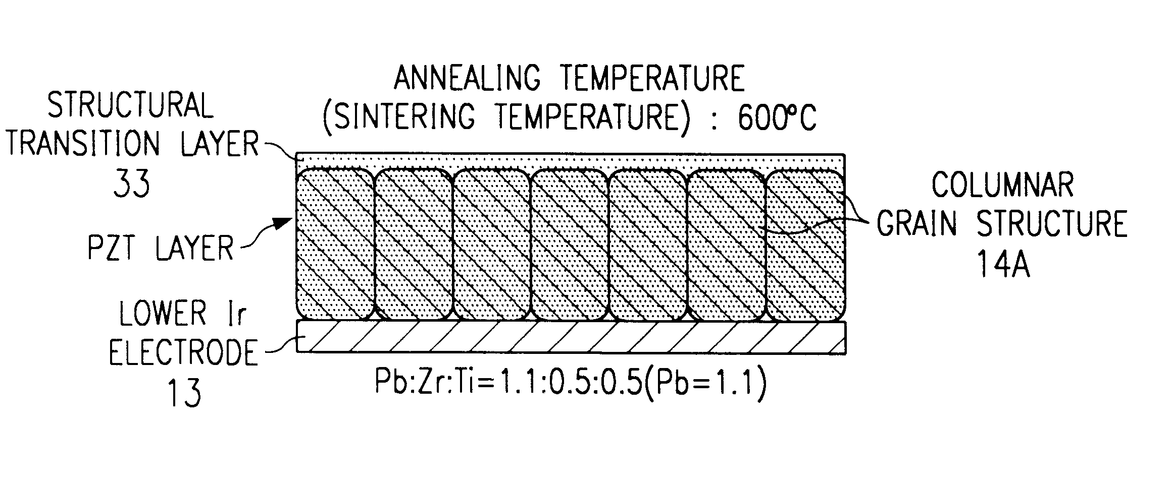
When a solution containing excess lead is used to form a PZT film with a perovskite crystal structure at a low temperature of 600.degree. C. or below, after the structural transition layer containing excess pB and formed on the PZT film is removed by means of dry etching, an upper electrode is formed on the PZT film. In this way, a ferroelectric capacitor free of polarization fatigue can be formed.
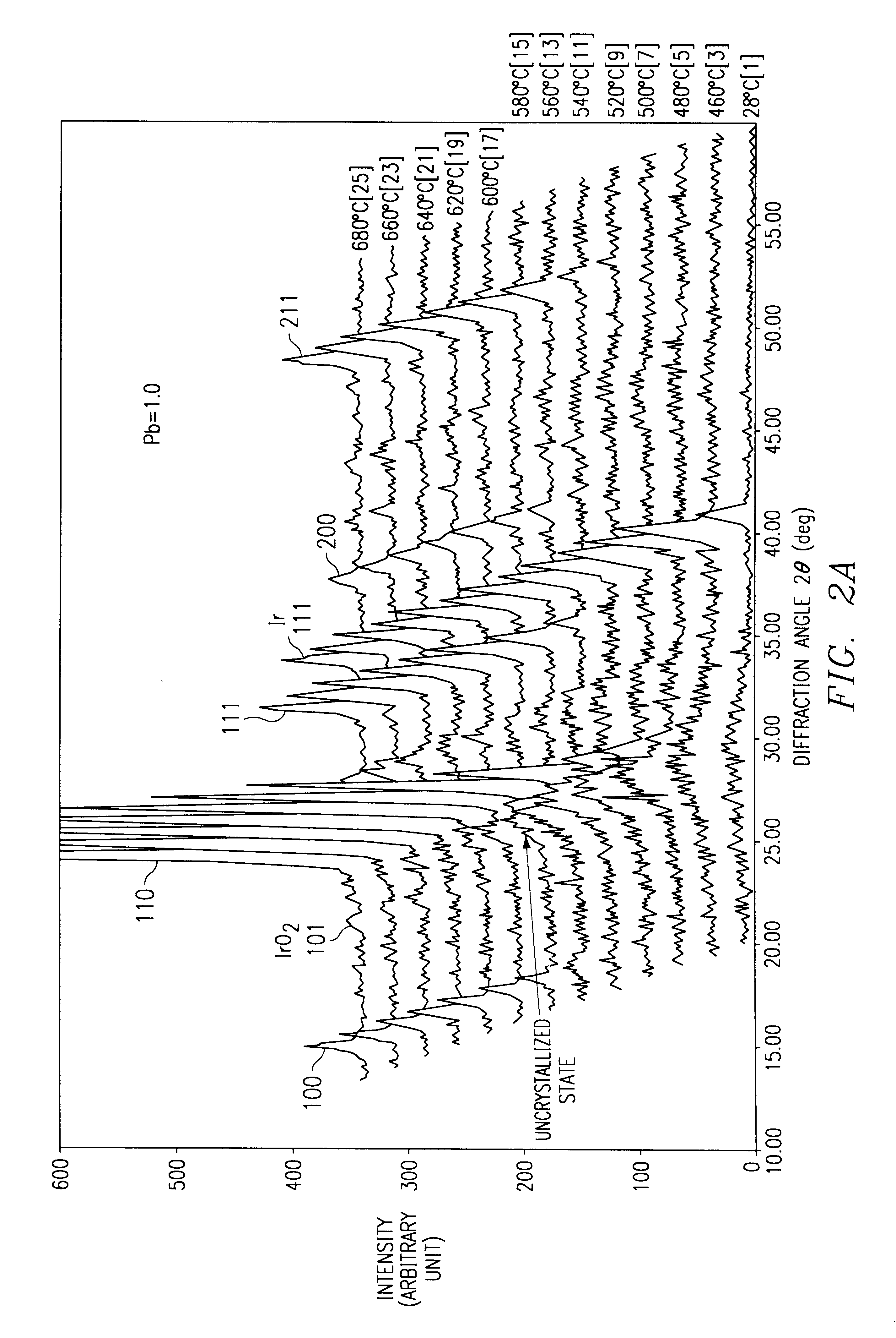
First, the crystallization temperature of PZT will be explained. Changes in the diffraction patterns during the crystallization process are observed by means of XRD (X-ray diffraction) for a PZT film made of a solution of a stoichiometric composition (Pb=1.0) and another PZT film made of a solution containing excess pB (Pb=1.2). The results of the observation are shown in FIG. 2. FIG. 3 shows the relationships of the crystallization starting temperature and ending temperature with the amount of Pb derived from ...
application examples
In the following, this invention will be explained in more detail with reference to embodiments.
first embodiment
FIGS. 1-14 show this invention.
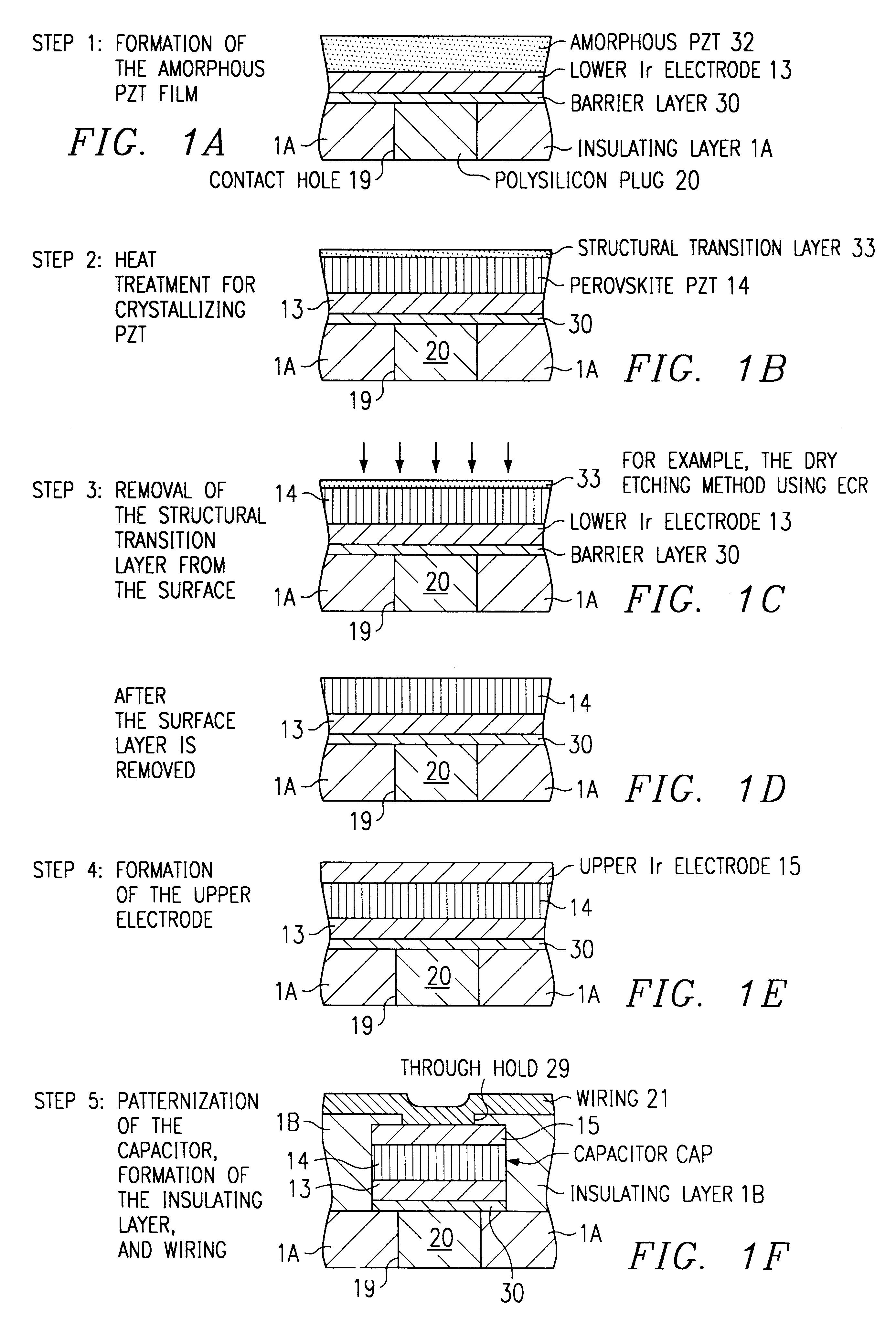
FIG. 1 is a diagram illustrating the process for forming a PZT capacitor using the method disclosed in this application example. In step 1, contact hole 19 is opened in insulating layer 1A, and an SiO.sub.2 film is formed on a Si wafer. Polysilicon plug 20 is formed selectively in the contact hole using the photolithography technology. A TiN film with a thickness of 200 nm is formed as barrier layer 30 (barrier metal) on the insulating layer using the reactive sputtering method. Lower electrode 13 with a thickness of 200 nm and made of Ir (iridium) is formed on the buffer layer using the sputtering or electron beam heating deposition method. Amorphous PZT film 32 with a thickness in the range of 200-500 nm is formed as the material of the sol-gel method on said lower Ir electrode 13 using the spin coating method. In this case, the composition of the sol-gel solution is Pb:Ti:Zr=1.2:0.5:0.5 (ratio of number of atoms) with a 20 atom % excess pB concentra...
PUM
| Property | Measurement | Unit |
|---|---|---|
| temperature | aaaaa | aaaaa |
| temperature | aaaaa | aaaaa |
| temperature | aaaaa | aaaaa |
Abstract
Description
Claims
Application Information


