Ceramic board for apparatuses for semiconductor manufacture and inspection

a ceramic board and semiconductor technology, applied in the direction of semiconductor/solid-state device testing/measurement, heater elements, transportation and packaging, etc., can solve the problems of poor temperature control characteristics, large thickness and bulk, metal heaters

Inactive Publication Date: 2002-11-05
IBIDEN CO LTD
View PDF18 Cites 98 Cited by
  • Summary
  • Abstract
  • Description
  • Claims
  • Application Information

AI Technical Summary

Benefits of technology

It is supposed that, in the present invention, complicated compounds such as Si--nitride component element (Al in the case of aluminum nitride)--O--N form in the grain boundaries of nitride ceramics to prevent decrease in Young's modulus at high temperature.
This is because by incorporating carbon in this manner, the ceramic board can be blackened and the radiant heat can be utilized with advantage when it is applied to a heater.
The carbon may be amorphous or crystalline. With amorphous carbon, the reduction in volume resistivity at elevated temperature can be prevented, while crystalline carbon is useful for preventing the reduction in thermal conductivity at high temperature. Therefore, depending on uses, both crystalline carbon and amorphous carbon may be used in a combination. The particularly preferred carbon content is 200 to 2000 ppm.

Problems solved by technology

However, metallic heaters have drawbacks such as poor temperature control characteristics, great thickness and bulk, and poor corrosion resistance to corrosive gases.
However, the experiments performed by the present inventors demonstrated that such aluminum nitrides suffer decreases in Young's modulus with increasing temperature.
With a declining Young's modulus, the incidence of curling at high temperature is increased so that wafers cannot be uniformly heated.

Method used


Image

  • Ceramic board for apparatuses for semiconductor manufacture and inspection
  • Ceramic board for apparatuses for semiconductor manufacture and inspection
  • Ceramic board for apparatuses for semiconductor manufacture and inspection

Examples


example 1

(1) Compositions of 1000 weight parts of aluminum nitride powder (average particle diameter: 1.1 .mu.m, Tokuyama), 4, 10, 20, 30, 40, 40, or 40 weight parts of yttria (average particle diameter: 0.4 .mu.m), 1.2.times.10.sup.-3, 4.8.times.10.sup.-3, 0.012, 0.027, 0.037, 0.050, or 0.074 weight parts of SiO.sub.2, 120 weight parts of acrylic binder, and the balance of alcohol were respectively spray-dried to provide 7 kinds of granular powders.

(2) Each of these granular powders was packed in a metal mold and formed into a plate (green). This green plate was drilled to form holes corresponding to the through-holes 95 for accepting wafer-supporting pins (diameter: 1.1 mm, depth: 2 mm) and holes 94 corresponding to the bottomed holes for embedding thermocouples therein.

(3) The green plate which had undergone the above processing was hot-pressed at a temperature of 1800.degree. C. and a pressure of 200 kg / cm.sup.2 to provide a 5 mm-thick aluminum nitride ceramic plate.

Then, a disk with a d...

example 2

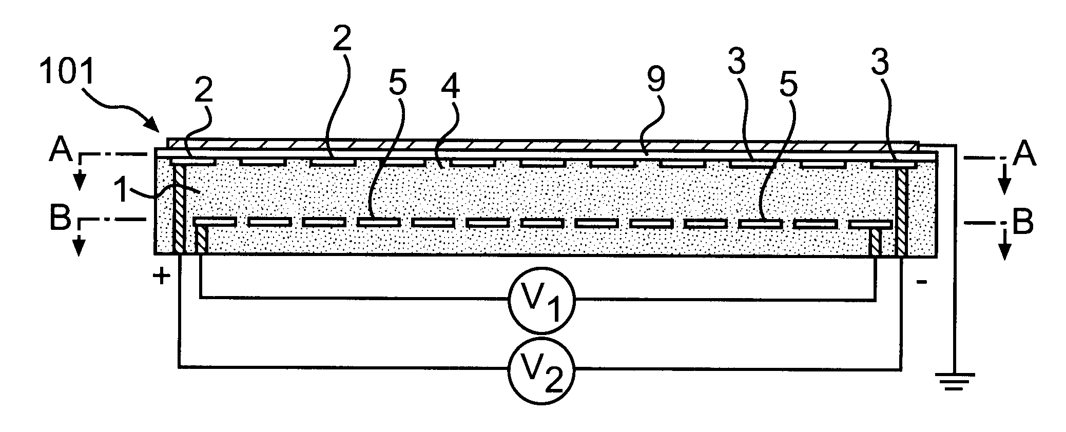
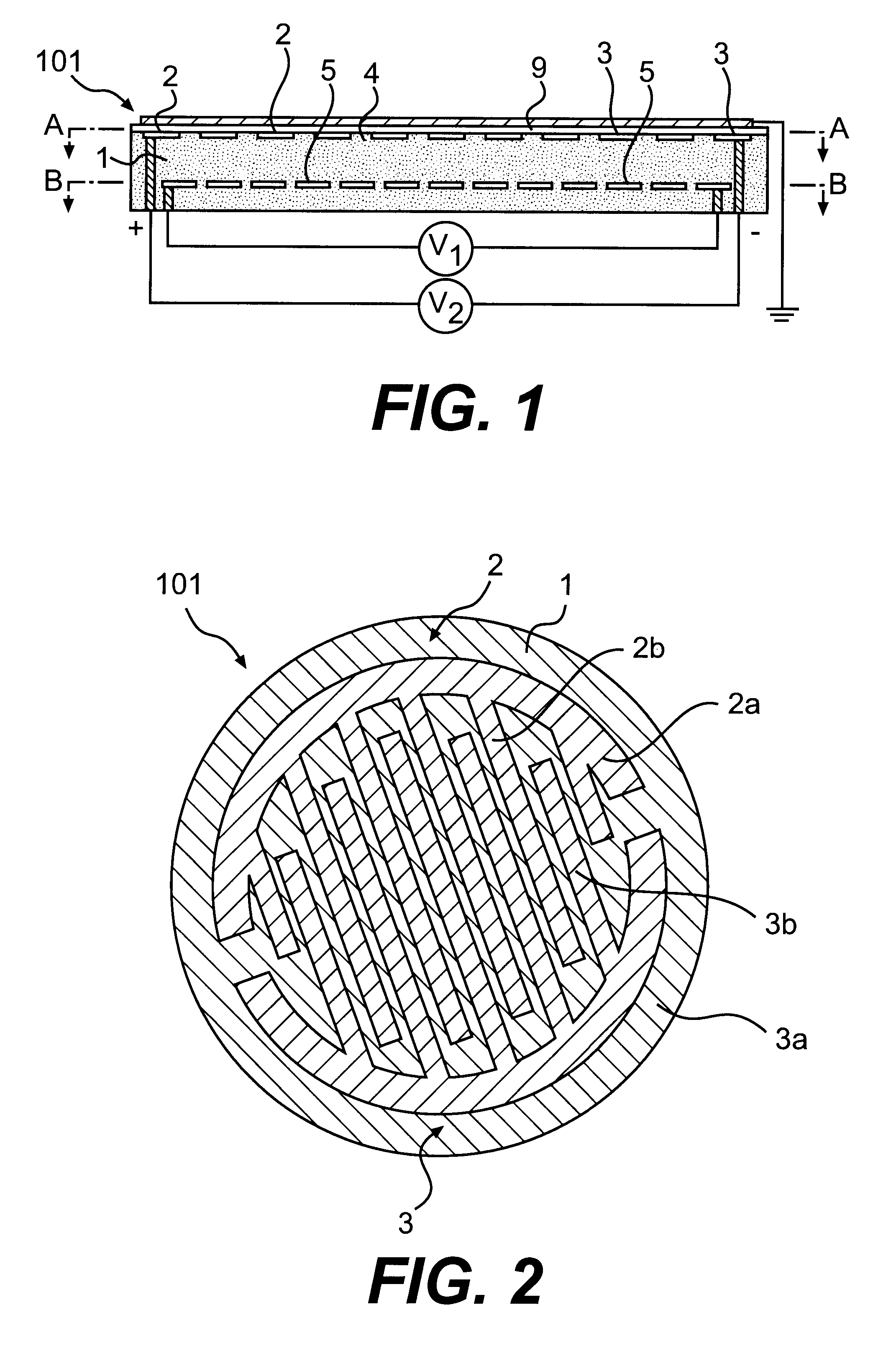
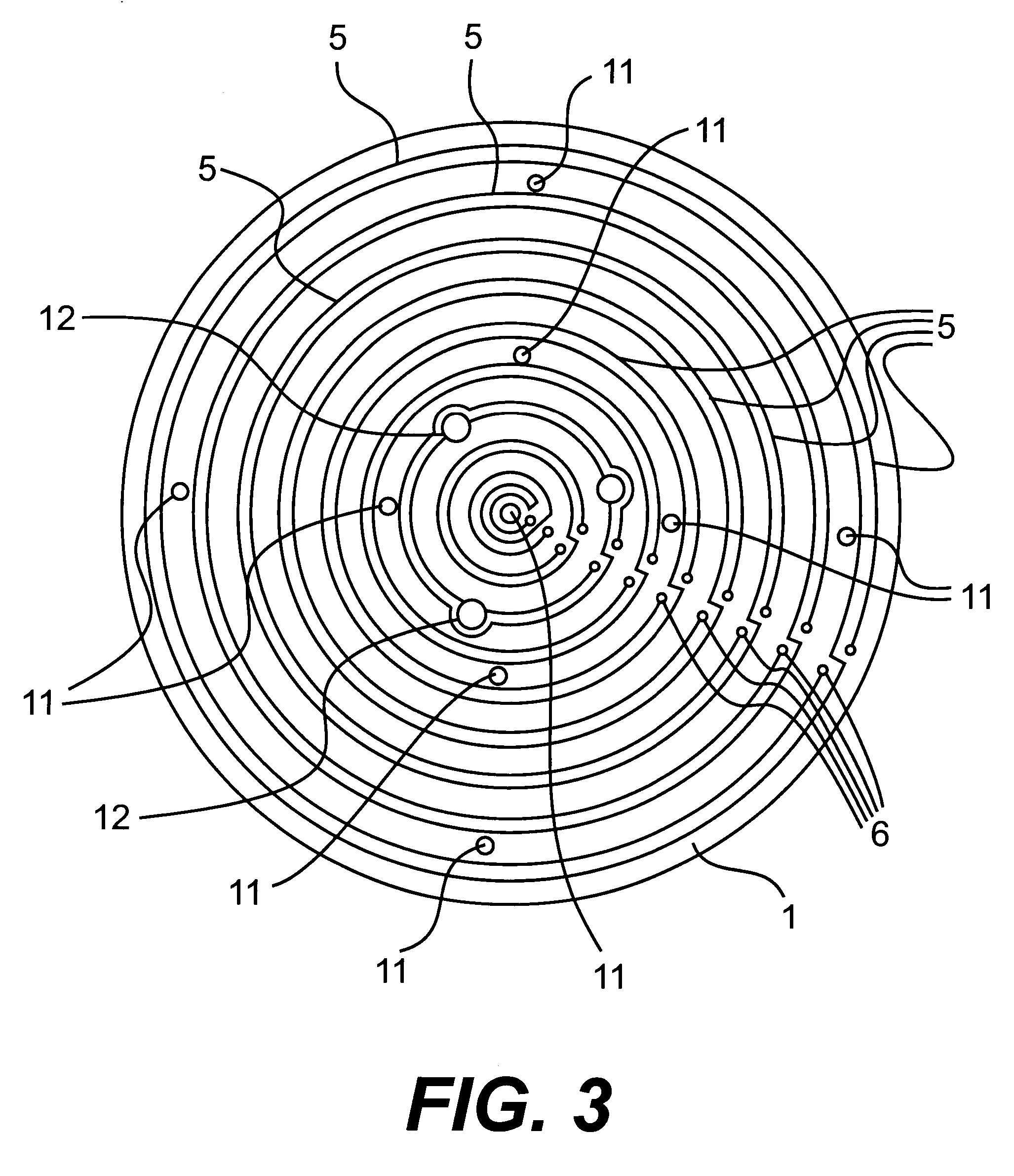
Manufacture of a Static Chuck (FIGS. 1 to 3)

(1) Using a paste comprising a mixture of 1000 weight parts of aluminum nitride powder (Tokuyama; average particle diameter: 1.1 .mu.m), 40 weight parts of yttria (average particle: diameter: 0.4 .mu.m), 0.027 weight parts of SiO.sub.2, 115 weight parts of acrylate binder, 5 weight parts of dispersant, 0.9 weight part of acrylic binder, 0.9 weight part of acrylic binder, and 530 weight parts of alcohol (1-butanol and ethanol), green sheets 50 having a thickness of 0.47 mm were molded by the doctor blade technique.

(2) After drying at 80.degree. C. for 5 hours, those green sheets 50 requiring processing were punch-formed with holes in the positions corresponding to the through-holes for accepting semiconductor wafer-supporting pins (1.8 mm, 3.0 mm, 5.0 mm in diameter) and holes in the positions corresponding to the plated-through holes for connecting external terminals.

(3) A conductive paste A was prepared by mixing 100 weight parts of a tun...

example 3

Manufacture of a Wafer Prover 201 (FIG. 6)

(1) A composition prepared by mixing 1000 weight parts of aluminum nitride powder (Tokuyama; average particle diameter: 1.1 .mu.m), 40 weight parts of yttria (average particle diameter: 0.4 .mu.m), 0.027 weight parts of SiO.sub.2 and 530 weight parts of alcohol (1-butanol and ethanol) was molded by the doctor blade technique to prepare green sheets having a thickness of 0.47 mm.

(2) Then, these green sheets were dried at 80.degree. C. for 5 hours and formed with punched through holes for plated-through holes for connecting the heating element to the external pins.

(3) A conductive paste A was prepared by mixing 100 weight parts of a tungsten carbide powder having an average particle diameter of 1 .mu.m, 3.0 weight parts of acrylic binder, 3.5 weight parts of .alpha.-terpineol as solvent, and 0.3 weight part of dispersant.

A conductive paste B was similarly prepared by mixing 100 weight parts of tungsten powder having an average particle diamete...


PUM

PropertyMeasurementUnit
thicknessaaaaaaaaaa
diameteraaaaaaaaaa
Young's modulusaaaaaaaaaa

Abstract

The present invention has for its object to inhibit decrease in Young's modulus at high temperature without compromise in various other characteristics such as heat conductivity.The present invention is directed to a ceramic board for semiconductor manufacture and inspection comprising a conductor layer internally or on the surface thereof which is composed of nitride ceramics containing oxygen and 0.1 to 50 ppm (wt.) of Si.

Description

The present invention relates to a ceramic board for the apparatuses used in-semiconductor manufacture and / or inspection, such as the hot plate (ceramic heater), static chuck and wafer prover.PRIOR ARTIn the semiconductor and / or inspection equipment inclusive of the etching and chemical vapor deposition lines, it is conventional to use heaters and wafer provers based on metallic substrates made of stainless steel, aluminum alloy or the like.However, metallic heaters have drawbacks such as poor temperature control characteristics, great thickness and bulk, and poor corrosion resistance to corrosive gases.To obviate those drawbacks, heaters based on ceramic boards such as aluminum nitride in lieu of metal substrates have heretofore been developed.Such ceramic heaters have the advantage that because of the high rigidity of the ceramic board itself, curling of the board, among other troubles, can be precluded without increasing the board thickness too much.As a technology of this type, ...

Claims


Application Information

Patent Timeline
Patent Type & Authority Patents(United States)
IPC IPC(8): C04B41/51C04B41/45C04B41/88H01L21/683H01L21/67C04B35/581C04B35/58H01L21/324H01L21/66H05B3/10H05K1/03
CPCC04B41/009C04B41/5116C04B41/88H01L21/6833C04B41/4539C04B35/581C04B2111/00844Y10T428/24926
Inventor NIWA, TAKEO
Owner IBIDEN CO LTD
Why Eureka
Try Eureka