Method of manufacturing a semiconductor device

a manufacturing method and semiconductor technology, applied in the direction of transistors, electrical devices, basic electric elements, etc., can solve the problems of not being able to use amorphous silicon film as an active layer, not being able to achieve good crystallinity of crystalline silicon film, and not being able to achieve the characteristics of a tft obtained by using crystalline silicon film

Inactive Publication Date: 2002-11-12
SEMICON ENERGY LAB CO LTD
View PDF19 Cites 134 Cited by
  • Summary
  • Abstract
  • Description
  • Claims
  • Application Information

AI Technical Summary

Problems solved by technology

Since such a driver circuit and a logic circuit are required to be operated at high speed, it is not suitable to use a noncrystalline silicon film (amorphous silicon film) as an active layer.
However, the crystallinity of the obtained crystalline silicon film is not so good.
The characteristics of a TFT obtained by using the crystalline silicon film also becomes unsatisfactory.
On the other hand, the method of heating has a problem that necessary crystallinity can not be obtained by a heat treatment at such a temperature that the glass substrate can withstand.
However, according to this method, the precipitation of grain boundaries is remarkable, and by this influence, the electrical characteristics of the obtained semiconductor device is not satisfactory.
Since such a metal element forms a deep level in a silicon film to capture a carrier, there is a fear that the metal element has a bad influence to the electrical characteristics and reliability of a TFT.

Method used


Image

  • Method of manufacturing a semiconductor device
  • Method of manufacturing a semiconductor device
  • Method of manufacturing a semiconductor device

Examples


embodiment 1

[Embodiment 1]

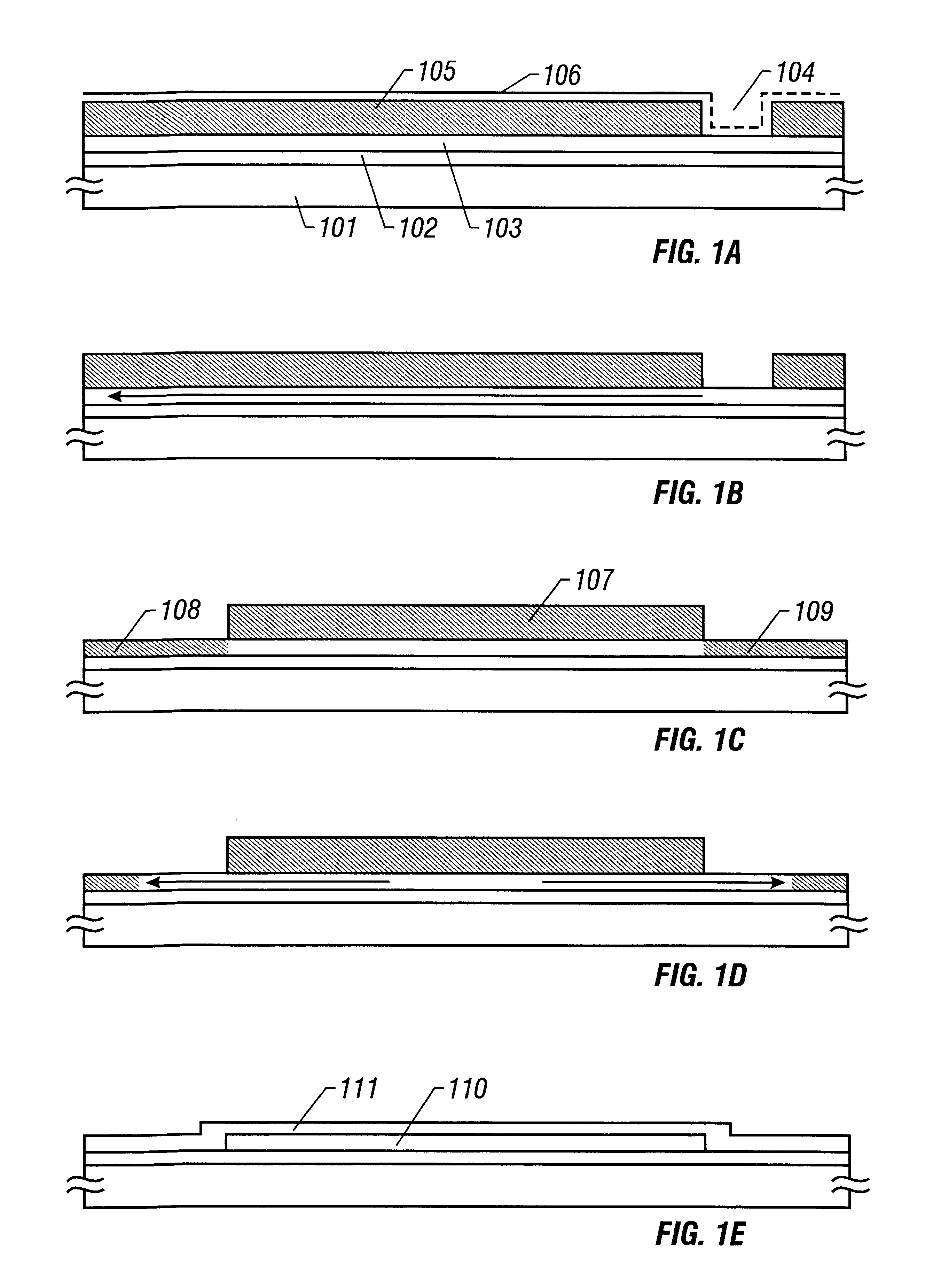
FIGS. 1A-1E and 2A-2D show manufacturing steps of this embodiment. In this embodiment, steps of manufacturing an N-channel TFT will be described.

First, as shown in FIG. 1A, a silicon oxide film 102 with a thickness of 400 nm as an under film is formed on a glass substrate 101 by a plasma CVD method. As the under film, a silicon nitride oxide film formed by a plasma CVD method or a silicon oxide film formed by a low pressure thermal CVD method may be used.

Other than the glass substrate, a quartz substrate may be used. A semiconductor substrate with a thermal oxidation film or a silicon oxide film formed on the surface thereof may also be used.

In this embodiment, an insulation substrate or a substrate having an insulating film will be referred to as a substrate having an insulating surface. Thus, the glass substrate 101 having the silicon oxide film 102 is also a substrate having an insulating surface. Of course, even if the silicon oxide film is not formed, the glass su...

embodiment 2

[Embodiment 2]

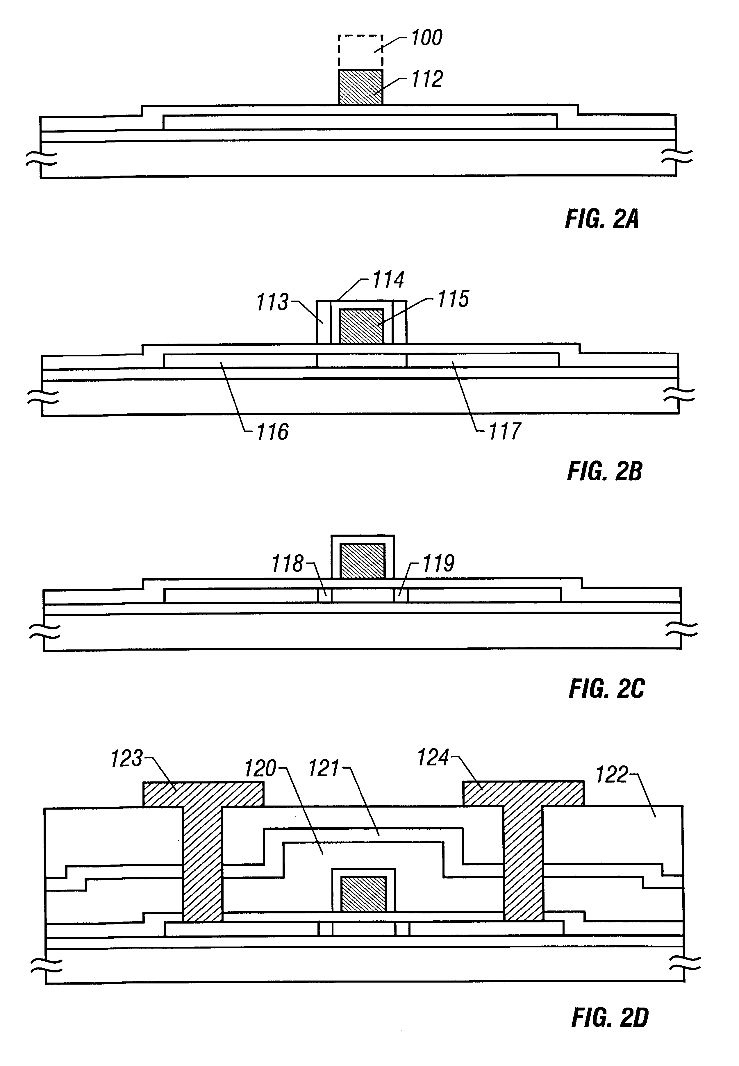
An example of manufacturing steps of forming an active layer made of a crystalline film by using the present invention will be described with reference to FIGS. 5A to 5F. In this example, nickel is used as a catalytic element, and phosphorus is used as an element for gettering.

First, a glass substrate 501 is prepared, and an under film 502 made of a silicon oxide film and having a thickness of 200 nm is formed thereon. Instead of the glass substrate, a quartz substrate, a silicon substrate, a ceramic substrate, and the like may be used.

Next, an amorphous silicon film 503 with a thickness of 10 to 75 nm (preferably 15 to 45 nm) is formed by using a plasma CVD method or a low pressure CVD method. Other than the amorphous silicon film, an amorphous semiconductor film comprising silicon, such as Si.sub.X Ge.sub.1-X (0

Next, a step of crystallizing the amorphous silicon film 503 is carried out. The detailed conditions are disclosed in Japanese Patent Unexam...

embodiment 3

[Embodiment 3]

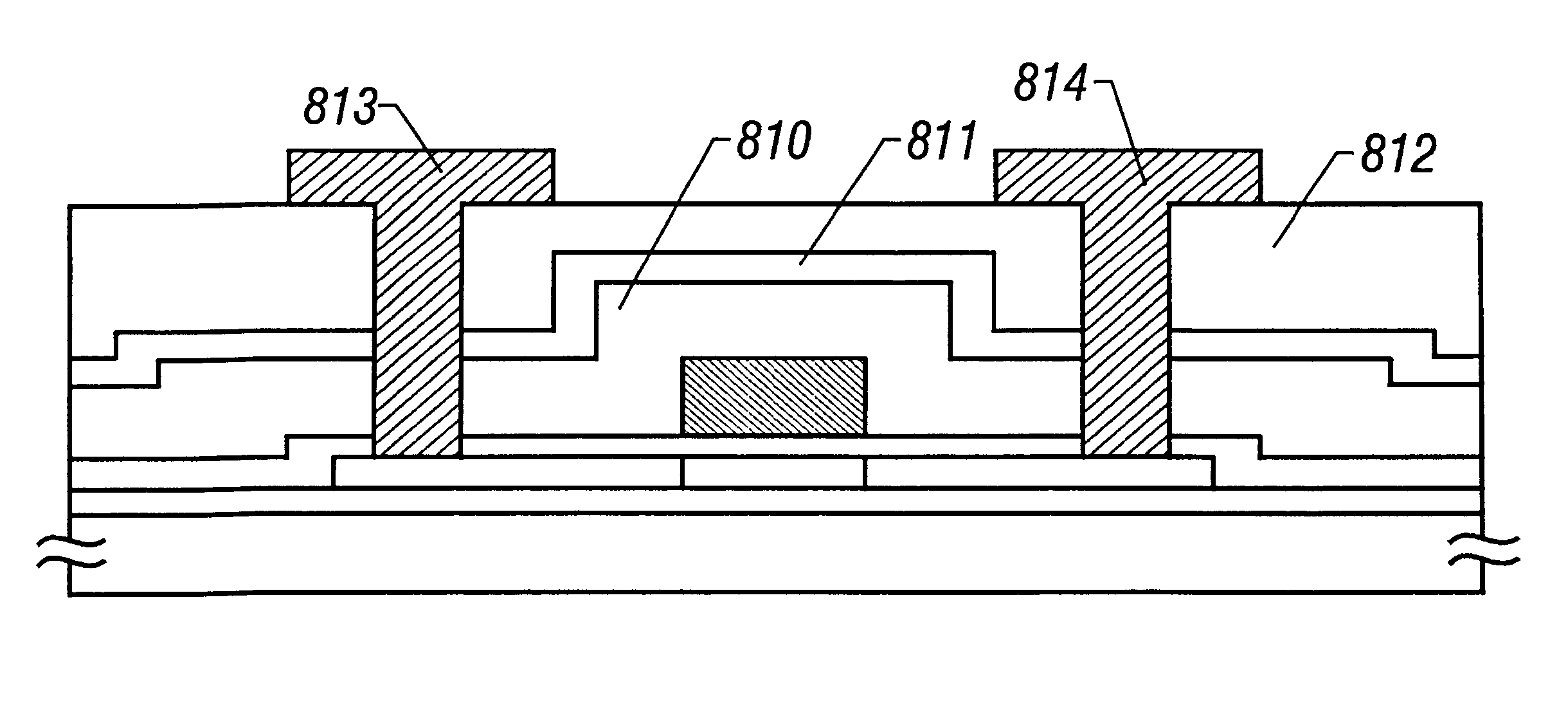
This embodiment is an example in which an ion implantation method is used as a method of introducing a nickel element in the step shown in embodiment 1 or embodiment 2.

When the nickel element is introduced by using the ion implantation method, it is possible to accurately control the amount of introduction. Further, since the size of the opening portion of the mask (for example, the portion 104 in FIG. 1) can be lessened to the order of .mu.m, it is possible to deal with the case where the circuit is made minute.


PUM

PropertyMeasurementUnit
temperatureaaaaaaaaaa
crystallization temperatureaaaaaaaaaa
thicknessaaaaaaaaaa

Abstract

A crystal growth 301 is carried out by diffusing a metal element, and a nickel element is moved into regions 108 and 109 which has been doped with phosphorus. An axis coincident with the moving directions 302 and 303 of the nickel element at this time is made to coincide with an axis coincident with the direction of the crystal growth, and a TFT having the regions as channel forming regions is manufactured. In the path of the region where nickel moved, since high crystallinity is obtained in the moving direction, the TFT having high characteristics can be obtained by this way.

Description

1. Field of the InventionThe present invention relates to a method of manufacturing a semiconductor device using a semiconductor thin film, and particularly to a method of manufacturing a thin film transistor (TFT) using a crystalline film containing silicon.Incidentally, the term "semiconductor device" used in the present specification includes all devices functioning by using a semiconductor, and not only a single element such as a TFT, but also an electro-optical device and an electronic device equipped therewith are also included in the category of the semiconductor device.2. Description of the Related ArtIn recent years, a technique of constituting a semiconductor circuit by forming TFTs on a glass substrate and the like, has been rapidly developed. As such a semiconductor circuit, an electro-optical device such as an active matrix type liquid crystal display device is typical.The active matrix type liquid crystal display device is a monolithic display device in which a pixel m...

Claims


Application Information

Patent Timeline
Patent Type & Authority Patents(United States)
IPC IPC(8): H01L21/02H01L21/20
CPCH01L21/2022H01L21/02488H01L21/02422H01L21/02532H01L21/0242H01L21/02672H01L21/02381H01L29/786
Inventor TAKANO, TAMAEOHNUMA, HIDETOOHTANI, HISASHINAKAJIMA, SETSUOYAMAZAKI, SHUNPEI
Owner SEMICON ENERGY LAB CO LTD
Why Eureka
Try Eureka