Semiconductor device structure with hydrogen-rich layer for facilitating passivation of surface states

a technology of surface state and device structure, which is applied in the direction of semiconductor devices, semiconductor/solid-state device details, electrical apparatus, etc., can solve the problems of data retention, data retention, and device standby power consumption, and the effect of reducing the power consumption of the devi

Inactive Publication Date: 2002-11-19
INFINEON TECH AG
View PDF8 Cites 90 Cited by
  • Summary
  • Abstract
  • Description
  • Claims
  • Application Information

AI Technical Summary

Problems solved by technology

Conventional fabrication techniques induce various forms of defect or damage to the layers within the device.
Recombination, particularly if it occurs at critical device interfaces such as isolation perimeters and gate oxides, results in leakage current.
Leakage current alters the gate threshold voltage, data retention, and standby power consumption of devices.
Thus, the presence of interface states adversely affects device functions.
However, current interconnection schemes and device structures tend to inhibit the ability of the hydrogen atoms from reaching the recombination sites to passivate the dangling bonds.
As such, the effectiveness and efficiency of the passivation anneal is reduced.
As known in the art, conventional device fabrication techniques damage chemical bonds, creating surface states at semiconductor interfaces.
However, current device structures tend to block hydrogen from reaching and passivating the surface states.
Percentages of hydrogen exceeding about 39% typically degrade the properties of the silicon nitride film, such as its ability to act as a barrier.
The oxynitride layer, when used as barrier liner, results in very low, reproducible STI bounded junction leakage for both the N and P diffusion.
It has been found that lower percentages of hydrogen bounded to silicon result in reduced junction leakage while higher percentages result in increased junction leakage.

Method used


Image

  • Semiconductor device structure with hydrogen-rich layer for facilitating passivation of surface states
  • Semiconductor device structure with hydrogen-rich layer for facilitating passivation of surface states
  • Semiconductor device structure with hydrogen-rich layer for facilitating passivation of surface states

Examples


example 1

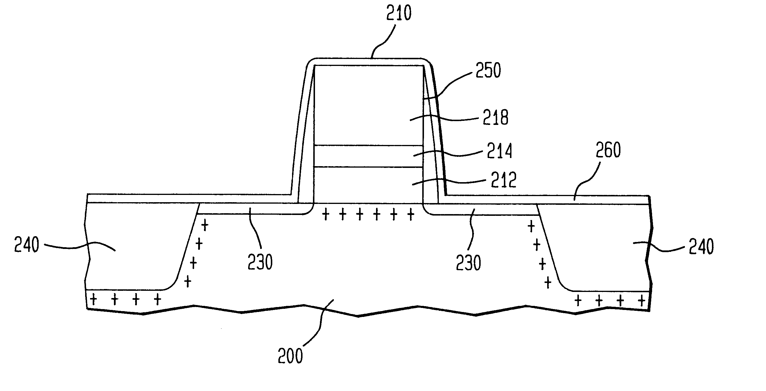
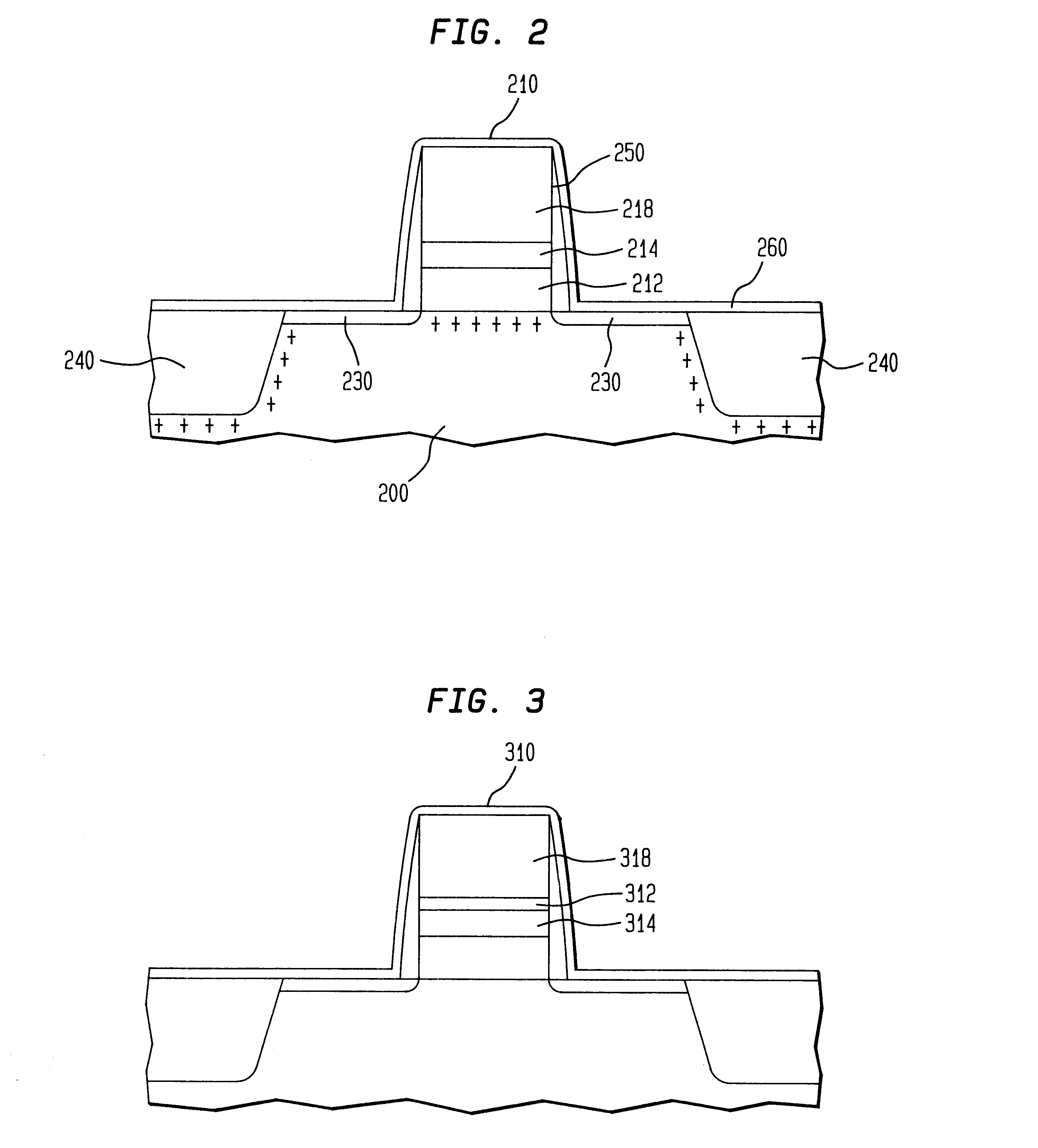
An experiment was conducted to compare leakage currents of devices incorporating the H-R silicon nitride layer against those with conventional silicon nitride layers. Eight lots (samples A-H) with devices fabricated thereon were prepared. The eight lots were processed in 2 different ways. Lots A-D comprise device structures fabricated with a conventional LPCVD silicon nitride layer to serve as a barrier or liner layer at the device interconnection interface. The device structures in lots A-D are similar to those described in FIG. 1. The conventional LPCVD silicon nitride film was deposited by reacting ammonia (NH.sub.3) with dichlorosilane (SiCl.sub.2 H.sub.2) in a furnace at about 720.degree. C. and 200 mTorr. The ratio of the NH.sub.3 to SiCl.sub.2 H.sub.2 is about 10:1. As for Lots E-H, the LPCVD nitride layer is replaced with an H-R silicon nitride layer, such as one described in FIG. 2. The H-R layer is deposited by PECVD in a reactor at about 480.degree. C., 5.75 Torr, and 340...

example 2

In FIG. 7, the characterization of PECVD H-R nitride films (samples A-C) was compared against that of an LPCVD nitride film. Sample A is a standard silicon nitride deposited by PECVD in a Novellus Concept-1 System. Sample B is a low SiH / UV PECVD nitride film deposited in a Novellus Concept-1 System. Both samples A and B were formed under similar conditions recommended by Novellus as described in "Users guide to 200 mm PECVD processing for the Novellus Concept One-200 mm Dielectric System" (published by Novellus Systems, Inc., of San Jose, Calif., 1992), which is herein incorporated by reference for all purposes. Sample C is an H-R silicon nitride film deposited by PECVD in an AME 5000 system from Applied Materials of Santa Clara, Calif. under similar conditions as the PECVD Film Lots (E-H) of Example 1. Sample D is a LPCVD nitride film deposited by LPCVD under similar conditions as the LPCVD film (Lots A-D) of Example 1.

After formation of the film, the samples were heated to 720.deg...

example 3

An experiment was conducted to analyze the relationship between SiH / (SiH+NH) and ND perimeter leakage using macros similar to those in the experiment of FIG. 5a-b. Data from the experiment are plotted in FIG. 8. As apparent from FIG. 8, lower concentrations of SiH / (SiH+NH) in the oxynitride film results in lower ND perimeter leakage. The ND leakage ranges from about 0.63 namp to about 1.72 namps for concentrations of SiH / (SiH+NH) ranging about 0-35%, respectively.


PUM


Abstract

A process for fabricating a device including the step of forming a structure for facilitating the passivation of surface states is disclosed. The structure comprises an oxynitride layer formed as part of the device structure. The oxynitride facilitates the passivation of surface states when heated.

Description

The invention generally relates to devices and device fabrication and, in particular, to devices having a layer for facilitating passivation of surface states and a process for fabricating such devices.BACKGROUND OF INVENTIONIn device fabrication, insulating, semiconducting, and conducting layers are produced and patterned on a substrate to form device structures, such as transistors, capacitors, or resistors. These device structures are then interconnected to achieve a desired electrical function. The production and patterning of the various device layers are achieved using conventional fabrication techniques such as, for example, oxidation, implantation, deposition, epitaxial growth of silicon, lithography and etching. Such techniques are described in S. M. Sze, "VLSI Technology", 2nd ed., New York, McGraw-Hill, 1988, which is herein incorporated by reference for all purposes.Conventional fabrication techniques induce various forms of defect or damage to the layers within the devi...

Claims


Application Information

Patent Timeline
Patent Type & Authority Patents(United States)
IPC IPC(8): H01L21/02H01L21/30H01L21/70H01L21/8242H01L21/28H01L21/314H01L21/318H01L27/108
CPCH01L21/28176H01L21/3003H01L21/3145H01L27/10873H01L27/10861H01L21/02274H01L21/0214H01L21/02304H01L21/02211H01L21/0217H10B12/038H10B12/05H01L21/31
Inventor COTE, DONNA RIZZONECOTE, WILLIAM JOSEPHNGUYEN, SON VANKIRCHHOFF, MARKUSLEVY, MAX G.HAUF, MANFRED
Owner INFINEON TECH AG
Why Eureka
Try Eureka