Method of forming buried wiring, and apparatus for processing substratum

a technology of substratum and buried wiring, which is applied in the direction of spraying apparatus, coatings, basic electric elements, etc., can solve the problems of difficulty in forming grooves and/or holes having a desired form in porous insulating layer under good control by dry etching method, and low mechanical strength of porous insulating layer, etc., to achieve high reliability and not damaged or broken

Inactive Publication Date: 2003-02-25
KOBE STEEL LTD
View PDF6 Cites 14 Cited by
  • Summary
  • Abstract
  • Description
  • Claims
  • Application Information

AI Technical Summary

Benefits of technology

It is therefore an object of the present invention to provide a method of forming a buried wiring, in which high reliability is accomplished, the wiring is neither damaged nor broken, an insulating layer used for burying the wiring is not damaged, and an insulating material can be reliably filled between the wirings.

Problems solved by technology

In the method using an insulating interlayer composed of a porous insulating layer, however, it is difficult to form a groove portion and / or a hole portion having a desired form in the porous insulating layer under good control by a dry etching method.
There is another problem that the porous insulating layer is damaged when a photoresist used in a lithography method is removed, so that the porous insulating layer is altered in chemical properties and form.
There is still another problem that, when a metal material and a barrier metal deposited on the porous insulating layer is removed by a CMP method, the porous insulating layer having low mechanical strength is broken due to a shear force exerted on the porous insulating layer.
However, this procedure involves a problem that the polishing rate of the metal material and the barrier metal deposited on the porous insulating layer is decreased, which results in a longer throughput.
Further, the hollow wiring method has the following problem when it is applied to an LSI wiring having a wiring line width of 1 .mu.m or less.
There may be therefore caused a phenomenon that the wiring line is mechanically deformed due to the above stress, which results in destruction.
Further, if the drying is made possible by taking measures against the surface tension, the following problem takes place.
As a result, the wiring lines vibrate, and when the vibration takes place intensely, the wiring lines may break due to the mechanical wearing of the wiring lines or a short circuit may be generated between the adjacent wiring lines.
These problems make it difficult to apply the hollow wiring method to fine wiring lines in which a distance between the wiring lines is small.
As a result, there is caused a problem that there is a region which is not filled with the insulating layer between the wiring lines.
Due to this problem, it is difficult to realize the technology of filling a hollow portion by removing the insulating layer in a gaseous phase and forming a new insulating layer in a gaseous phase.
Further, there is another problem that a device isolation region and a gate insulating layer of a transistor portion are damaged with an etching gas used for removing the insulating layer by a dry etching method.

Method used


Image

  • Method of forming buried wiring, and apparatus for processing substratum
  • Method of forming buried wiring, and apparatus for processing substratum
  • Method of forming buried wiring, and apparatus for processing substratum

Examples


example 1

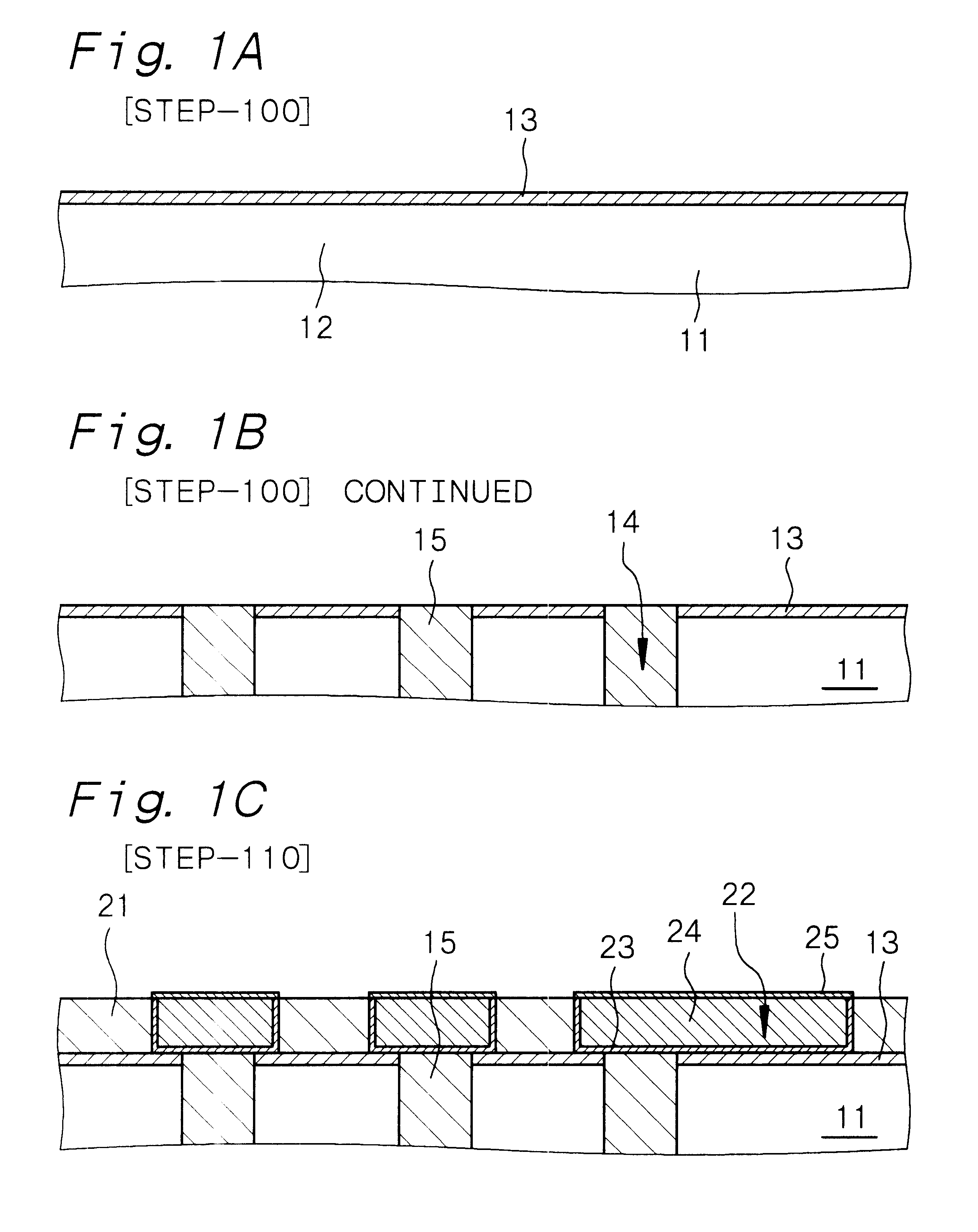
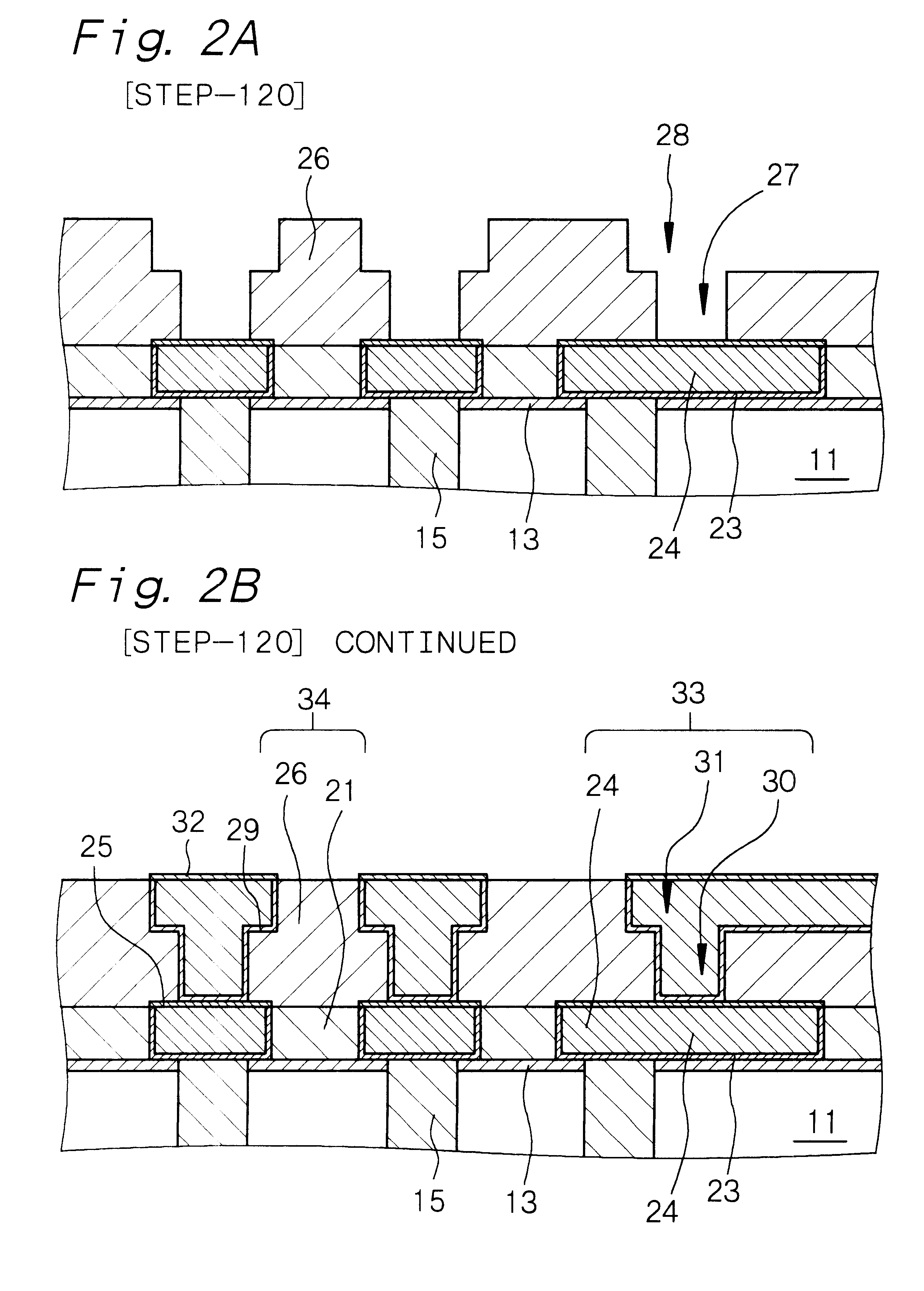
is concerned with a method of forming a buried wiring, provided by the present invention. The method of forming a buried wiring in Example 1 will be explained with reference to FIGS. 1A, 1B, 1C, 2A, 2B, 3A, 3B, 4A, 4B, 5A and 5B showing schematic partial cross-sectional views of a substratum and the like.

[Step-100]

First, a semiconductor device such as a transistor and a lower wiring layer (these are now shown) are formed in or on a semiconductor substrate (not shown), and then, a lower insulating layer 12 is formed thereon. The lower insulating layer 12 corresponds to a substratum 11. Then, a protective insulating layer 13 for protecting the lower insulating layer 12 from a fluid (first-insulating-layer dissolving fluid) to be used for dissolving a first insulating layer in a step to come later is formed on the lower insulating layer 12, for example, by a CVD method (see FIG. 1A). The protective insulating layer 13 is composed of silicon nitride (SiN). Then, a hole portion 14 is for...

example 2

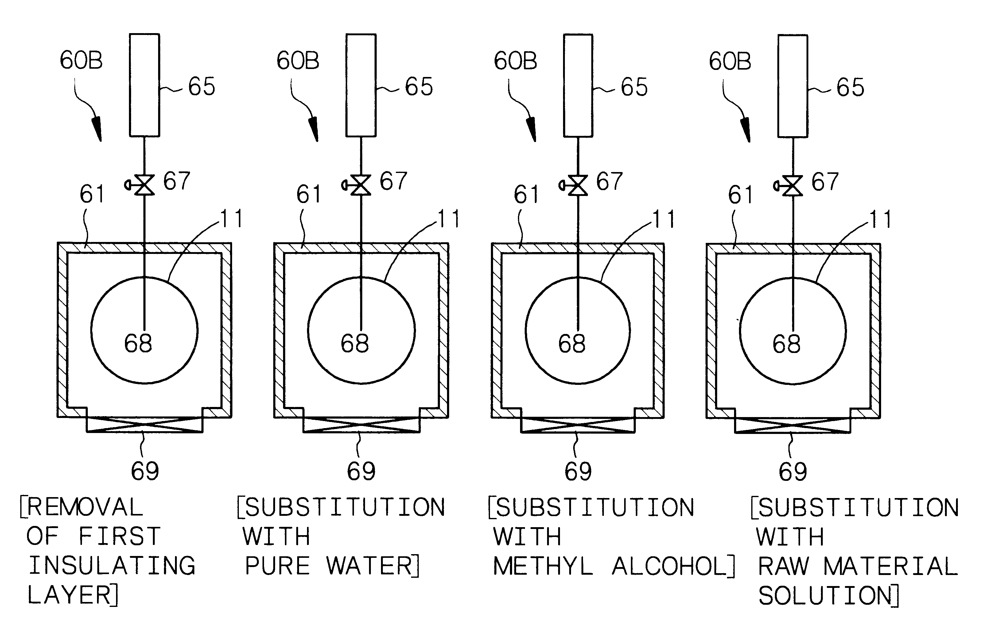
is concerned with the first-structured apparatus for constituting the apparatus for processing a substratum of the present invention. The first-structured apparatus will be referred to as "first processing apparatus" hereinafter. The first processing apparatus of Example 2 is a single wafer processing apparatus, which can be used for carrying out the steps (B) and (C) and the step of filling the second insulating layer formed by gelation in the raw material solution at least between the wirings (to be referred to as "filling step in the step (D)" hereinafter) out of the step (D) in the method of forming a buried wiring in the present invention.

FIG. 6 shows a conceptual view of the first processing apparatus 60 of single wafer processing apparatus type, in which the first-insulating-layer removing means and the raw-material-solution substituting means are constituted of one process chamber 61. The process chamber 61 has a substratum supporting stage 62 and a substratum transfer porti...

example 3

Example 3 is concerned with the second-structured apparatus for constituting the apparatus for processing a substratum of the present invention. The second-structured apparatus will be referred to as a "second processing apparatus" hereinafter. The second processing apparatus of Example 3 is a single wafer processing apparatus, and the steps (B) and (C) and the filling step in the step (D) in the method of forming a buried wiring in the present invention are carried out with separate second processing apparatus.

Each of the first-insulating-layer removing means and the raw-material-solution substituting means has a process chamber 61; a substratum supporting stage 62 which is disposed in the process chamber 61 and is used for supporting a substratum 11 thereon; a substratum transfer portion 69 provided in the process chamber 61; a fluid supply source 65 of a fluid for dissolving the first insulating layer or processing fluids for carrying out various processes (these fluids will be s...


PUM

PropertyMeasurementUnit
relative dielectric constantaaaaaaaaaa
widthaaaaaaaaaa
temperatureaaaaaaaaaa

Abstract

A method of forming a buried wiring comprising the steps of: (A) forming a wiring and a first insulating layer filled between the wirings on a substratum, (B) immersing the first insulating layer in a fluid which can dissolve the first insulating layer, to dissolve the first insulating layer into the fluid, (C) substituting, for the fluid, a raw material solution containing a raw material for forming a second insulating layer, without bringing the wiring into contact with a gas, and (D) filling a second insulating layer formed by gelation in the raw material solution at least between the wirings, and then, drying off the raw material solution, thereby to form the second insulating layer at least between the wirings.

Description

BACKGROUND OF THE INVENTION AND RELATED ART STATEMENTThe present invention relates to a method of forming a buried wiring and an apparatus for processing a substratum.Studies are being vigorously made for decreasing a dielectric constant of an insulating interlayer used in a semiconductor device.As one of the methods for decreasing the dielectric constant, studies are being made on the application of a porous insulating layer to an insulating interlayer. Having a low relative dielectric constant (.epsilon.), a porous insulating layer is expected to be promising as a raw material for decreasing a capacitance between wiring lines. In principle, a porous insulating layer is conventionally formed by a process of forming a porous structure having solid linkages on the basis of a solidification reaction according to dehydration / condensation in an aqueous solution containing tetraethoxysilane (TEOS) and ammonia (NH.sub.3), and then drying off the aqueous solution.And, a metal wiring is for...

Claims


Application Information

Patent Timeline
Patent Type & Authority Patents(United States)
IPC IPC(8): H01L21/02H01L21/70H01L21/768H01L21/316H01L21/283H01L23/522
CPCH01L21/02126H01L21/02203H01L21/02216H01L21/02282H01L21/02304H01L21/31695H01L21/76801H01L21/7682H01L21/76826H01L21/76885H01L21/02343H01L2221/1047H01L21/283
Inventor NOGAMI, TAKESHIKOMAI, NAOKIIKEDA, KOICHIKINOSHITA, TAKASHISUZUKI, KOHEIKAWAKAMI, NOBUYUKIFUKUMOTO, YOSHITO
Owner KOBE STEEL LTD
Why Eureka
Try Eureka