Multi-layered wiring layer and method of fabricating the same

a wiring layer and multi-layer technology, applied in the direction of semiconductor devices, semiconductor/solid-state device details, electrical apparatus, etc., can solve the problems of difficult to make diffusion-barrier films, copper is more corrosive than aluminum, and difficult to dry-etch copper

Inactive Publication Date: 2003-03-25
GK BRIDGE 1
View PDF7 Cites 69 Cited by
  • Summary
  • Abstract
  • Description
  • Claims
  • Application Information

AI Technical Summary

Problems solved by technology

However, since copper does not form passive state composed of an oxide film, at a surface thereof, unlike aluminum, copper is more corrosive than aluminum.
It is quite difficult to dry-etch copper, and hence, a copper wiring layer is formed generally by chemical mechanical polishing (CMP).
However, the conventional barrier film for preventing copper diffusion is accompanied with the following problems.
The first problem is that it is quite difficult to make a diffusion-barrier film have both a characteristic of preventing copper diffusion and a sufficient adhesive force with copper.
The second problem is caused when a diffusion-barrier film is designed to have a multi-layered structure in order to avoid the above-mentioned problem of the single-layered diffusion-barrier film.
However, since it was not possible in a conventional method to successively form a crystalline metal film and an amorphous metal nitride film by sputtering, the crystalline metal film and the amorphous metal nitride film had to be separately formed in the same sputtering chamber or be formed in separate sputtering chambers.
However, in accordance with this method, the titanium nitride film cannot be formed until partial pressures of argon and nitrogen become stable by varying a mixture ratio of argon and nitrogen.
Hence, it is impossible to enhance a fabrication yield of fabricating a diffusion-barrier film having a multi-layered structure.
The third problem relates to coverage of a film formed by sputtering.
Since metal particles sput

Method used


Image

  • Multi-layered wiring layer and method of fabricating the same
  • Multi-layered wiring layer and method of fabricating the same
  • Multi-layered wiring layer and method of fabricating the same

Examples


second example

FIG. 9 shows a relation between a flow rate ratio and resistivity of a film formed by high-pressure RF magnetron sputtering having been explained in the first example, for various RF powers. Herein, the flow rate ratio is defined as a ratio of a volume of argon gas to be introduced into the chamber 21 to a volume of nitrogen gas to be introduced into the chamber 21 (N.sub.2 / (Ar+N.sub.2)).

The relation shown in FIG. 9 was observed when the chamber 21 had a pressure of 13 Pa, the semiconductor substrate 22 was heated at 200 degrees centigrade, the permanent magnets 24 were rotated at 10 r.p.m., and the distance between the metal target 28 and the semiconductor substrate 22 was 134 mm.

As a ratio of N.sub.2 gas in the flow rate ratio N.sub.2 / (Ar+N.sub.2) is increased, the resistivity is once reduced, and thereafter, increased again, regardless the RF power. However, an increase rate of the N.sub.2 gas ratio is dependent on the RF power. The resistivity increases at a lower rate at the ...

third example

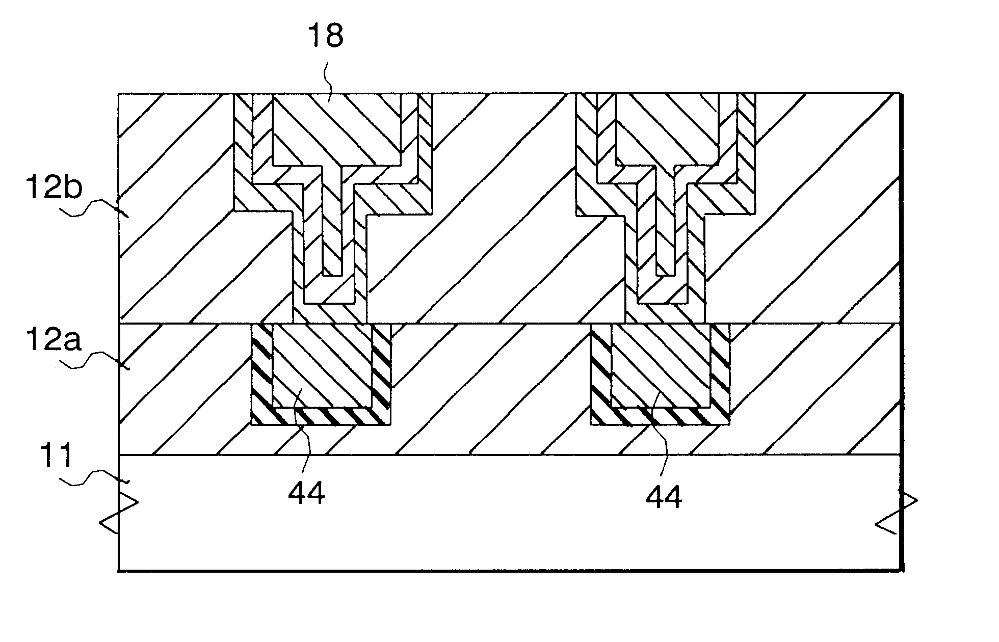
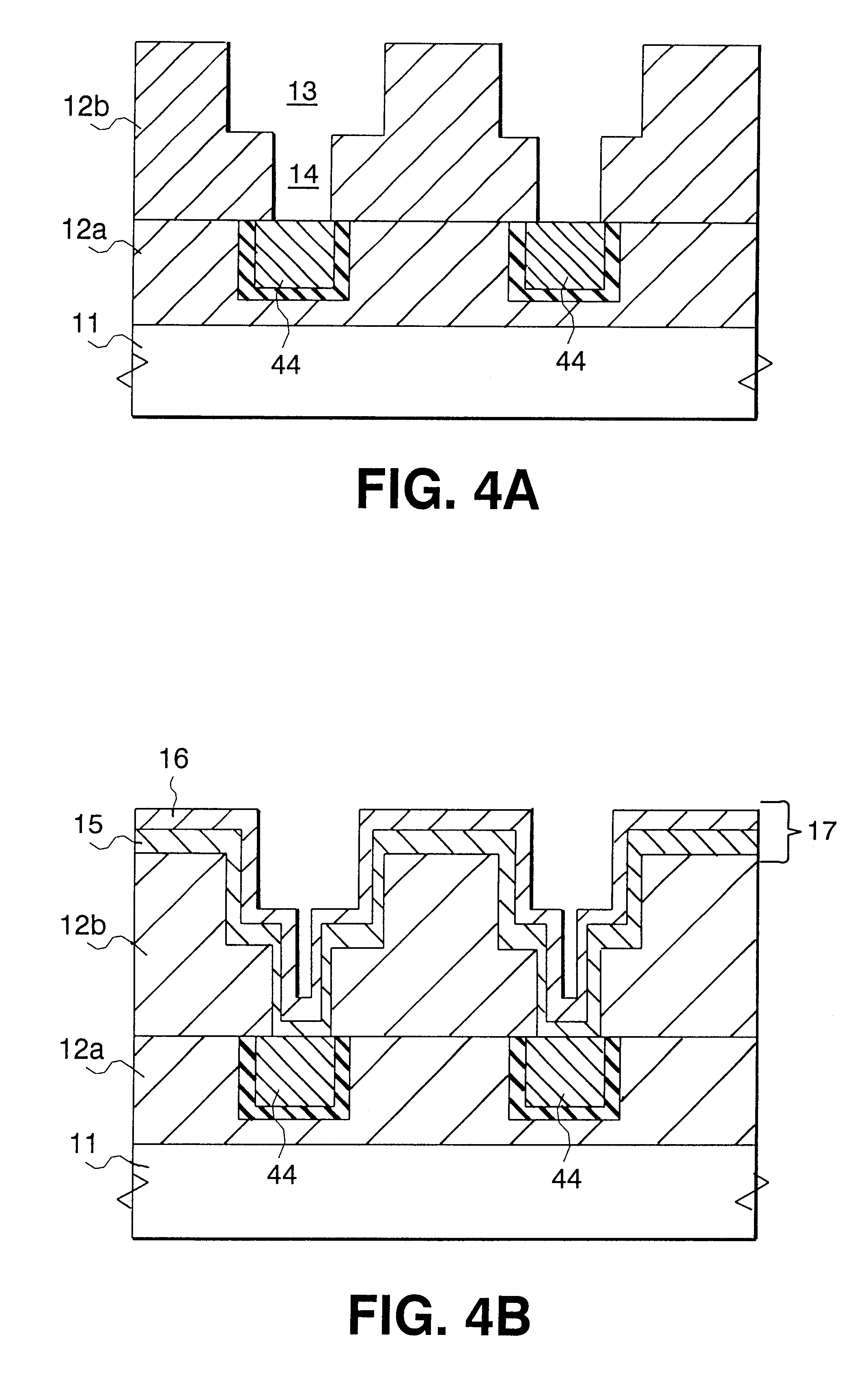
The RF magnetron sputtering having been explained in the first example makes it possible to enhance coverage characteristic of a deposited film for covering a recess or hole therewith, by introducing a gas having a higher pressure than usual, specifically, a pressure equal to or greater than 5 Pa, into a chamber. That is, it is possible to form the multi-layered barrier film 17 under desired coverage characteristic by switching RF power with a sputtering pressure being kept equal to or greater than 5 Pa, even when there is carried out dual-damassin process in which the recess 13 and the hole 14 formed at a surface of the second insulating film 12b formed on the semiconductor substrate 11 are concurrently filled with the diffusion-barrier film 17.

fourth example

In the above-mentioned first and second examples, the process in which a multi-layered barrier film is successively formed by switching RF power while the film is being formed is applied to RF magnetron sputtering. This process may be applied to DC magnetron sputtering, as illustrated in FIG. 24, though a N.sub.2 gas ratio and RF power are different from those in the first and second examples.

FIG. 24 illustrates a DC magnetron sputtering apparatus. The apparatus is comprised of a chamber 21, a heater 34 fixed on a bottom of the chamber 21 for heating a semiconductor substrate 22, a target metal 28 fixed to a top of the chamber 21 by means of insulators 29 and a cathode 23, a pump 33 for exhausting air from the chamber 21 such that a pressure in the chamber 21 is in the range of about 1.times.10.sup.-7 Pa to about 1.times.10.sup.-6 Pa, a magnet 42 positioned above the target metal 28, mass flow controllers 31 for adjusting flow rates of argon gas and nitrogen gas, and allowing the ga...


PUM


Abstract

There is provided a barrier film preventing diffusion of copper from a copper wiring layer formed on a semiconductor substrate. The barrier film has a multi-layered structure of first and second films wherein the first film is composed of crystalline metal containing nitrogen therein, and the second film is composed of amorphous metal nitride. The barrier film is constituted of common metal atomic species. The barrier film prevents copper diffusion from a copper wiring layer into a semiconductor device, and has sufficient adhesion characteristic to both a copper film and an interlayer insulating film.

Description

1. Field of the InventionThe invention relates to a semiconductor integrated circuit including a copper wiring layer, and more particularly to a barrier film which prevents copper diffusion from such a copper wiring layer.2. Description of the Related ArtAs a semiconductor device has been designed to be smaller and smaller in size, wiring delay exerts greater influence on a silicon ULSI device. As a result, though a wiring layer has been composed of aluminum, it is necessary to compose a wiring layer of copper in place of aluminum.Resistivity of copper is equal to about 70% of resistivity of aluminum. However, since copper does not form passive state composed of an oxide film, at a surface thereof, unlike aluminum, copper is more corrosive than aluminum.In addition, since copper has a high diffusion rate in both silicon (Si) and silicon dioxide (SiO.sub.2), if copper enters MOSFET formed on a silicon substrate, copper would induce reduction in carrier lifetime.Hence, it is absolutel...

Claims


Application Information

Patent Timeline
IPC IPC(8): H01L21/02H01L21/70H01L23/532H01L21/768H01L21/285H01L23/522H01L23/52H01L21/28H01L21/3205
CPCH01L21/2855H01L21/76846H01L21/76862H01L21/76865H01L23/5226H01L23/53238H01L2924/0002H01L2924/3011H01L2924/00
Inventor TAGAMI, MASAYOSHIHAYASHI, YOSHIHIRO
Owner GK BRIDGE 1
Why Eureka
Try Eureka