High speed semiconductor memory device with short word line switching time

a semiconductor memory and line switching technology, applied in semiconductor devices, digital storage, instruments, etc., can solve the problems of difficult to precisely establish the timing between the read timing of the memory cell, and the increase in the delay time of the sense amplifier, so as to improve the operation speed of the sense amplifier and reduce the access time and cycle time of the memory cell. , the effect of improving the operation speed

Inactive Publication Date: 2003-03-25
VACHELLIA
View PDF5 Cites 32 Cited by
  • Summary
  • Abstract
  • Description
  • Claims
  • Application Information

AI Technical Summary

Benefits of technology

To reduce the memory cell access time and the cycle time in the semiconductor memory, it is effective to improve the operation speed of the sense amplifier for amplifying the read signal from the memory cell, for example. A latch type sense amplifier for am

Problems solved by technology

However, if the latch activation signal SALAT is retarded unnecessarily to avoid this erroneous operation, the delay time of the sense amplifier increases.
This problem results after all in the problem how to establish timing between the data read out from the memory cell and the latch activation signal of the sense amplifier.
However, it is difficult to precisely establishing the timing between the read

Method used


Image

  • High speed semiconductor memory device with short word line switching time
  • High speed semiconductor memory device with short word line switching time
  • High speed semiconductor memory device with short word line switching time

Examples


first embodiment

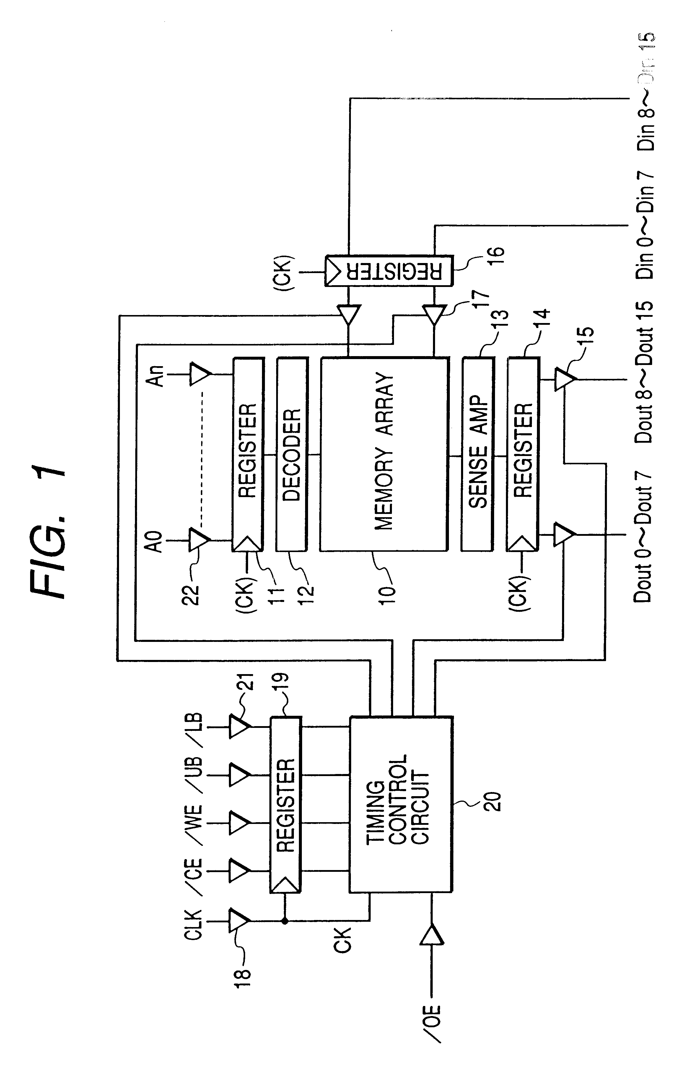
FIG. 1 is a schematic structural view showing a clock synchronization type static RAM to which the present invention is applied appropriately.

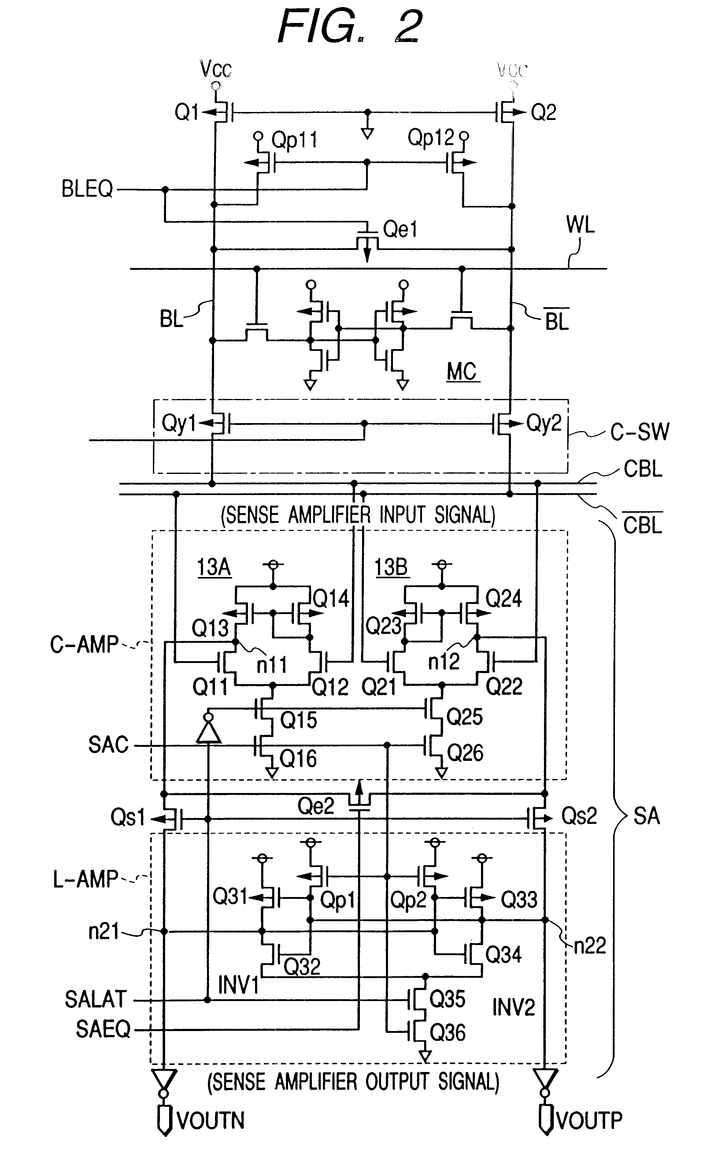
Referring to FIG. 1, reference numeral 10 denotes a memory array that has a plurality of memory cells disposed in matrix, a plurality of word lines to which selection terminals of the memory cells of the same row are connected, and a plurality of bit lines to which input / output terminals of the memory cells of the same column are connected. Reference numeral 11 denotes an address register for latching input address signals A0 to An in synchronism with a clock signal CK. Reference numeral 12 denotes an address decoder for decoding the latched address signal and selecting the corresponding word line inside the memory array 10. Reference numeral 13 denotes a sense amplifier line comprising a plurality of sense amplification circuits each being disposed for each bit line pair to which the selected memory cell is connected, and for amplifying a pot...

second embodiment

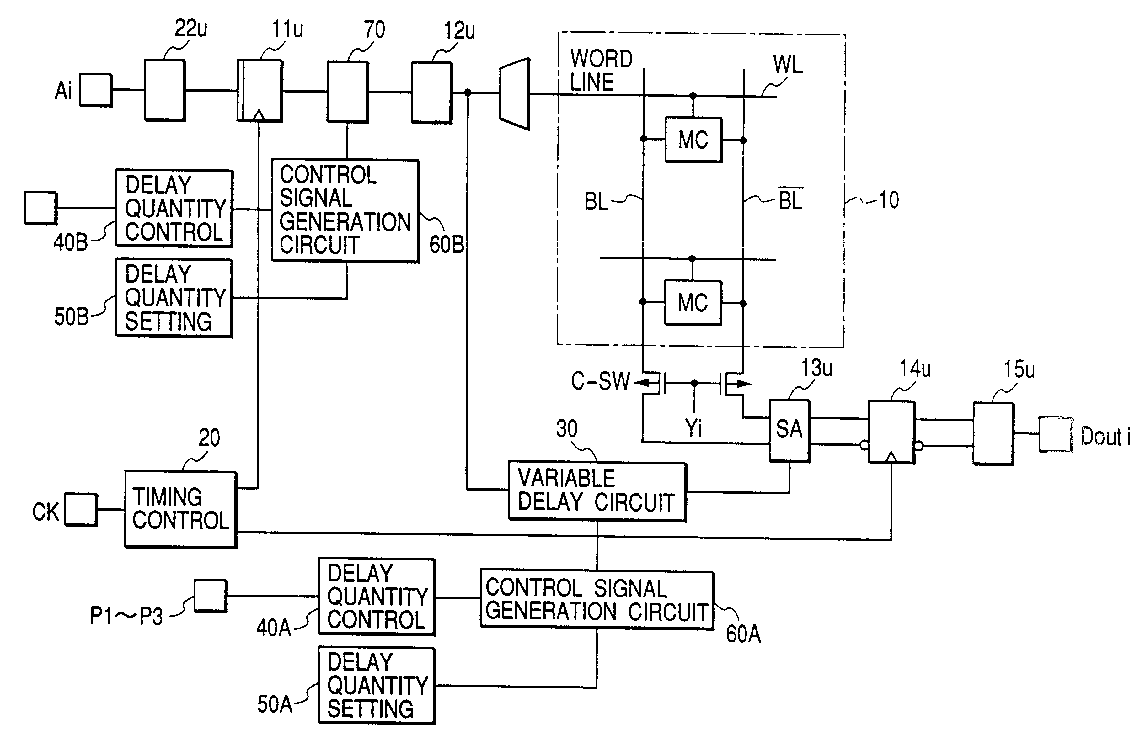
In this second embodiment, the variable pulse generation circuit 70 is interposed between the address register 11u and the address pre-decoder 12u as shown in FIG. 9. The variable pulse generation circuit 70 renders the fall of the internal address signal supplied to the pre-decoder 12u. In this way, a signal having a variable pulse width is generated. In order to vary the pulse width in this variable pulse generation circuit 70 and to conduct the test of the memory, this embodiment includes a second delay quantity controlling circuit 40B, a second delay quantity setting circuit 50B for setting the delay quantity determined on the basis of the test result and a second control signal generation circuit 60B for generating a control signal for the variable pulse generation circuit 70.

The variable pulse generation circuit 70 is the one that has substantially the same circuit construction as the variable delay circuit 30 in the first embodiment shown in FIG. 5. The second delay quantity ...

fourth embodiment

In this fourth embodiment, the control signal / WE representing the data read or write operation is supplied to the variable pulse generation circuit 70" through the buffer 21u so that the pulse width (select time) can be changed between the data read operation and the data write operation as shown in FIG. 14. To independently adjust the pulse width of the word line between the read operation and the write operation, this embodiment includes a third delay quantity controlling circuit 40C, a third delay quantity setting circuit 50C and a third control signal generation circuit 60C, each being for the write operation and corresponding to the second delay quantity controlling circuit 40B, the second delay quantity setting circuit 50B and the second control signal generation quantity 60B for the read operation, besides these circuits 40B, 50B and 60B.

Incidentally, the word line select time must be shorter in the data write operation than in the data read operation. However, since the rec...


PUM


Abstract

Setting means (such as fuse circuits) for adjusting the timings of various signals such as an activation timing of a sense amplifier, a fall timing of a word line, a recovery operation (equalization) of a bit lines and so forth, checking an operation in a test stage of a chip, and permanently programming (fixing) the timing of an internal signal to the condition of the highest operation speed that can be confirmed as acquirable in this check stage, is provided.

Description

This invention relates to a technology for improving an operation speed of a semiconductor memory device. More particularly, this invention relates to a technology that will be effective when used for semiconductor memory devices for which a high-speed operation is required, such as a clock synchronization type SRAM (Static Random Access Memory) and a dynamic RAM.A memory access time and a cycle time are two important performance factors that determine high-speed performance of semiconductor memory devices such as SRAM (hereinafter called merely the "semiconductor memory" or the "memory"). The term "memory access time" means the time necessary for an address signal, a clock signal, etc, that are inputted from outside the memory to flow through a path for selecting the memory cell and to output desired data. The term "cycle time" means the time of the minimum cycle in which operations such as read and write operations can be executed normally.FIG. 16 shows the construction of a synch...

Claims


Application Information

Patent Timeline
IPC IPC(8): G11C7/22G11C8/08G11C8/00G11C7/10G11C7/00G11C11/413G11C29/00G11C11/407G11C11/417G11C11/419H01L21/822H01L27/04
CPCG11C7/1072G11C7/22G11C11/413G11C8/08G11C2207/2281G11C29/00
Inventor AKIOKA, TAKASHISHINOZAKI, MASAO
Owner VACHELLIA
Why Eureka
Try Eureka