Method to selectively cap interconnects with indium or tin bronzes and/or oxides thereof and the interconnect so capped

a technology of indium or tin bronze and/or tin bronze, which is applied in the manufacture of printed circuits, conductive pattern reinforcements, basic electric elements, etc., can solve the problems of shortening of solutions, and fewer metal deposits, so as to prevent uncontrollable growth of copper corrosion products

Inactive Publication Date: 2003-04-22
GLOBALFOUNDRIES INC
View PDF12 Cites 24 Cited by
  • Summary
  • Abstract
  • Description
  • Claims
  • Application Information

AI Technical Summary

Benefits of technology

The invention also provides layers of indium or tin bronzes as barriers to the electromigration of copper. The m

Problems solved by technology

These solutions are subject to shorting across very finely-spaced interconnects.
Relatively few metals can be deposited by an immersion process, mainly because of standard potential mismatch.
(U.S. Pat. No. 5,364,459) requires titanium salts many of which are regulated by the Toxic Substances Control Act and are likely to present disposal issues.
However, each of these described systems is limited to plating a layer of metal.
The problem of plating a layer of alloy wa

Method used


Image

  • Method to selectively cap interconnects with indium or tin bronzes and/or oxides thereof and the interconnect so capped
  • Method to selectively cap interconnects with indium or tin bronzes and/or oxides thereof and the interconnect so capped
  • Method to selectively cap interconnects with indium or tin bronzes and/or oxides thereof and the interconnect so capped

Examples


Embodiment Construction

.

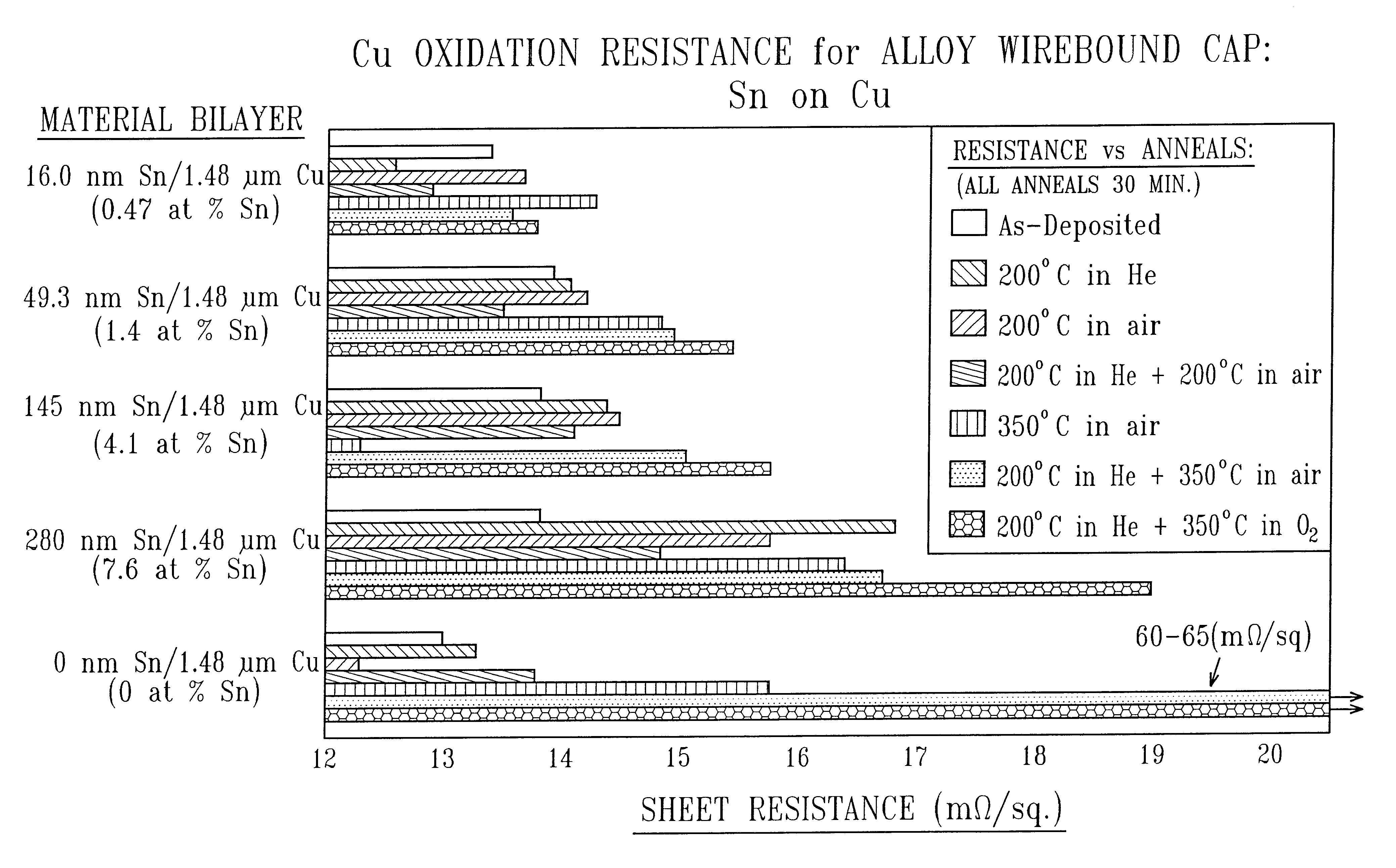
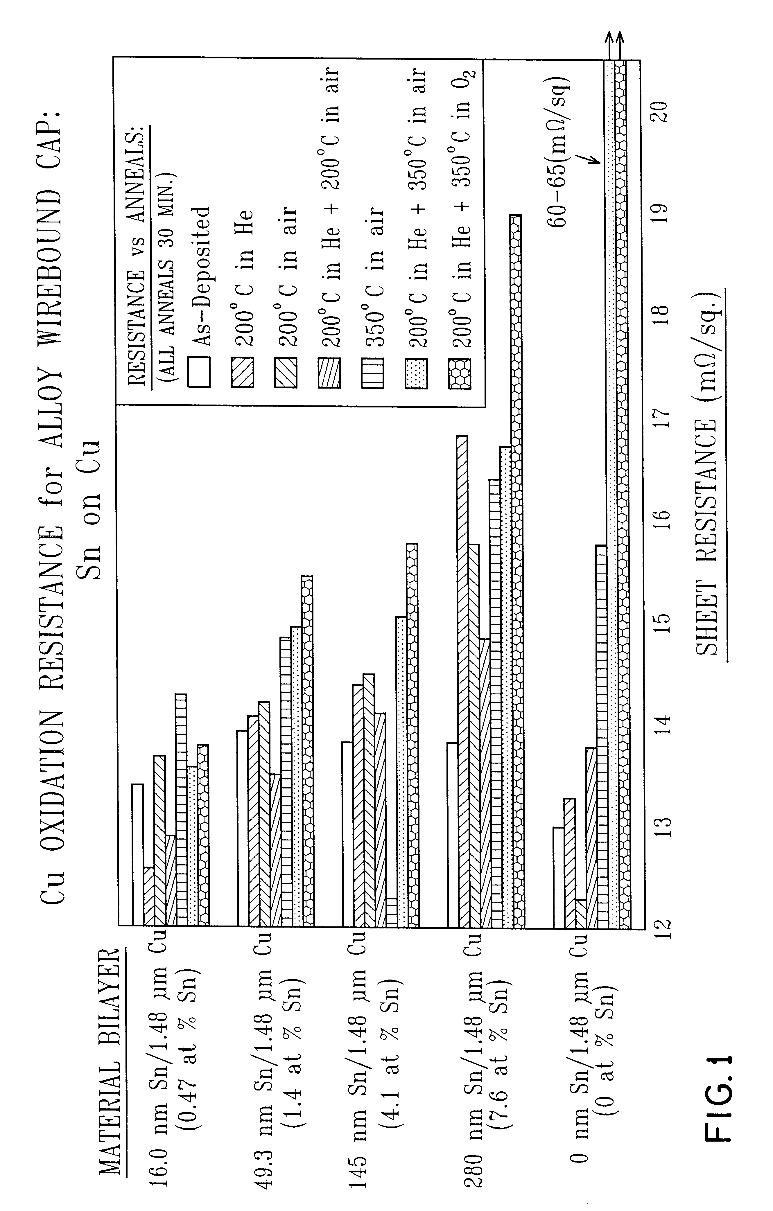
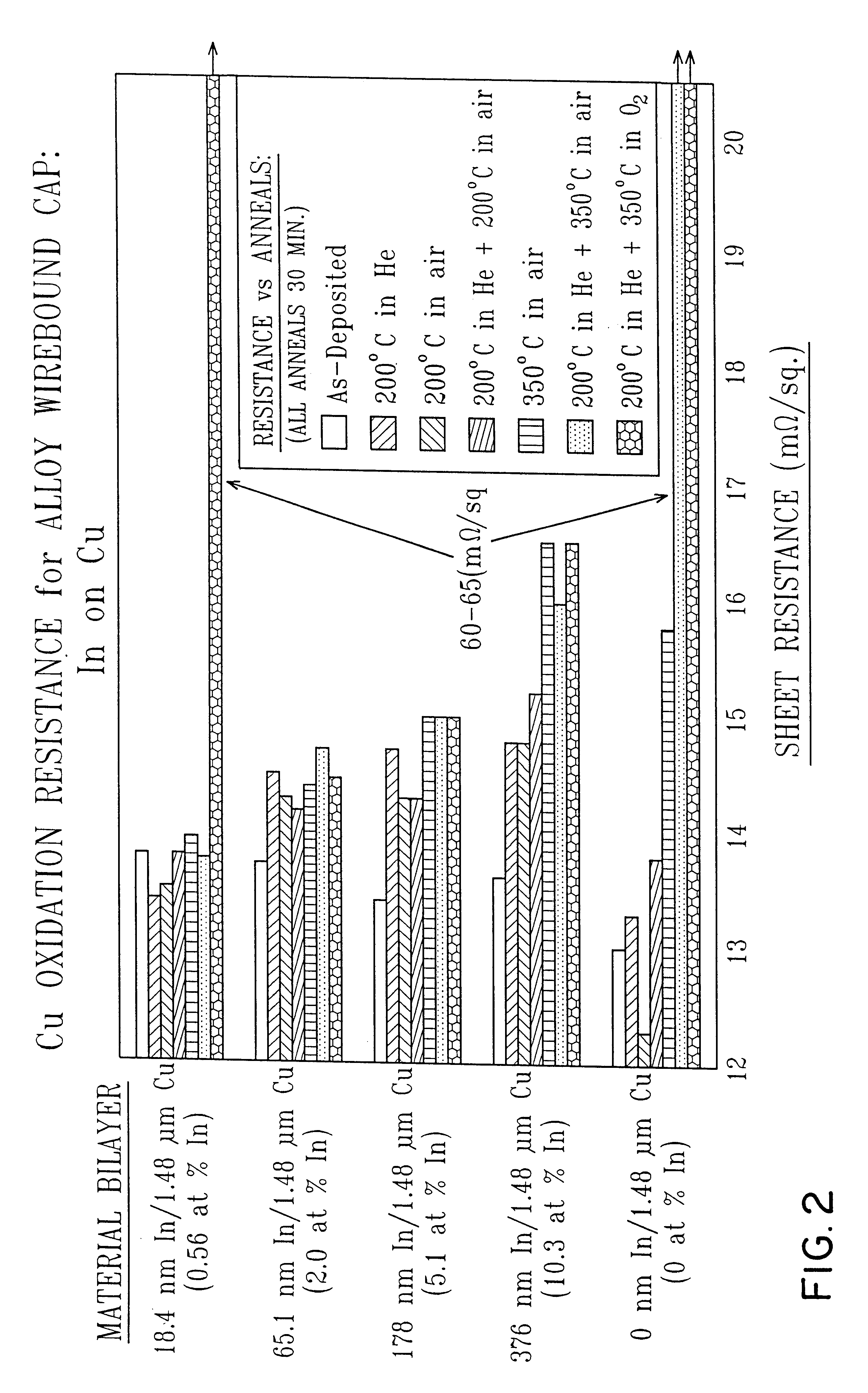
Reference is made to the figures to illustrate selected embodiments and preferred modes of carrying out the invention. It is to be understood that the invention is not hereby limited to those aspects depicted in the figures. One embodiment of the invention can be understood with reference to FIG. 7 which schematically depicts the process sequence of the present invention. Shown is an interconnect provided by a standard damascene, or dual damascene fabrication process with electroplated Cu fill 3, where 1 is a SiO.sub.2 or other appropriate substrate and 2 is a liner. See Edelstein et al., "Full Copper Wiring in Sub-0.25.mu.m CMOS Technology", Tech. Digest IEEE Int. Electron Devices Mtg., 776 (1997) disclosure of which is herein incorporated by reference. At the stage following CMP planarization, the Cu interconnects are encapsulated on three sides by a refractory liner, but the upper surface is exposed. Subsequent processing steps that attack or corrode Cu may not be used. Were a r...


PUM


Abstract

A method to selectively cap interconnects with indium or tin bronzes and copper oxides thereof is provided. The invention also provides the interconnect and copper surfaces so formed.

Description

The present invention relates generally to the specifically directed plating of indium and tin bronzes on copper structures, and particularly, but not by way of limitation, to coating the top surface of semiconductor interconnects with an indium, or tin bronze or an oxide thereof. The invention also relates to the interconnect so formed.It is desirable to selectively cap copper interconnects with an alloy coating to provide improved adhesion, electromigration resistance, redundant current-strapping, improved via contact resistance, robustness, and corrosion protection. The capping must be highly selective, specifically plating only the copper wiring, so as not to require expensive and critical lithography and etching to define the cap over the interconnect and to remove it from the spaces between interconnects. Cu on-chip contacts (e.g. wire bond or C4 pads) need similar capping for robust, corrosion-resistant terminal metallurgical contact. Previously, this problem has been address...

Claims


Application Information

Patent Timeline
IPC IPC(8): H01L23/52H01L21/768H01L21/288H01L23/532H01L21/02H01L21/60H01L21/70H05K3/24
CPCH01L21/2885H01L21/76856H01L21/76858H01L21/76862H01L23/53238H01L24/11H05K3/244H01L21/76849H01L2224/0401H01L2224/04042H01L2224/05546H01L2224/13099H01L2924/01013H01L2924/0102H01L2924/01022H01L2924/01029H01L2924/01049H01L2924/01078H01L2924/01079H01L2924/01082H01L2924/01327H01L2924/01005H01L2924/01006H01L2924/01023H01L2924/01033H01L2224/45144H01L2924/15747H01L2924/00
Inventor EDELSTEIN, DANIEL C.KANG, SUNG KWONMCGLASHAN-POWELL, MAURICEO'SULLIVAN, EUGENE J.WALKER, GEORGE F.
Owner GLOBALFOUNDRIES INC
Why Eureka
Try Eureka