Integrated scheme for predicting yield of semiconductor (MOS) devices from designed layout

a technology of integrated schemes and semiconductors, applied in individual semiconductor device testing, semiconductor/solid-state device testing/measurement, instruments, etc., can solve problems such as catastrophic failure, device variability and product yield loss of semiconductor devices, and degrade transistor parameters, so as to reduce device variability

Inactive Publication Date: 2003-05-13
MONTEREY RES LLC +2
View PDF5 Cites 74 Cited by
  • Summary
  • Abstract
  • Description
  • Claims
  • Application Information

AI Technical Summary

Benefits of technology

FIG. 24 is an illustration of retargeting the process to take advantage of reduced device variability due to OPC or process improvement.
The present invention bridges the gap between photolithographic simulations and determination of device yield. The present invention includes determining statistics of at least one MOSFET parameter, from the gate pattern derived by photolithographic simulations. The statistics of one or more MOSFET parameters may then be used to determine device yield.

Problems solved by technology

Within-chip variability of critical features such as polycrystalline silicon (poly) lines due to limitations of manufacturing processes is a major cause of device variability and product yield loss in semiconductor devices.
In particular, optical proximity effects on the poly layer can degrade transistor parameters or even lead to catastrophic failures, such as shorts or opens.
Gate length variability is the main source of circuit-level variation and a major performance and yield limiter.
Optical Proximity Correction serifs (or hammerheads) that enhance pattern resolution on wafers for deep submicron layouts are particularly vulnerable to the quality of the mask making process.
Also, the designed serif size, often much smaller than that of MOSFET channels and connecting lines, is close to the mask resolution limits and therefore difficult to control.
The differences between the drawn and on-mask serif size and shape, as well as intramask variation, may no longer guarantee transistor performance within specified limits.
While the latitude of such a process could impact transistor parameters, no work has been done to link its accuracy to the final yield loss due to MOSFET degradation.
The photolithographic simulations (drawing of pattern, optical simulation, and determination of gate pattern) could not be easily, or previously coupled with systems for determining device yield (determining MOSFET parameters, then determining device yield from the parameters) because there was no way to transform the results of the photolithographic simulations into a form usable by the software for determining device yield.

Method used


Image

  • Integrated scheme for predicting yield of semiconductor (MOS) devices from designed layout
  • Integrated scheme for predicting yield of semiconductor (MOS) devices from designed layout
  • Integrated scheme for predicting yield of semiconductor (MOS) devices from designed layout

Examples


example 1

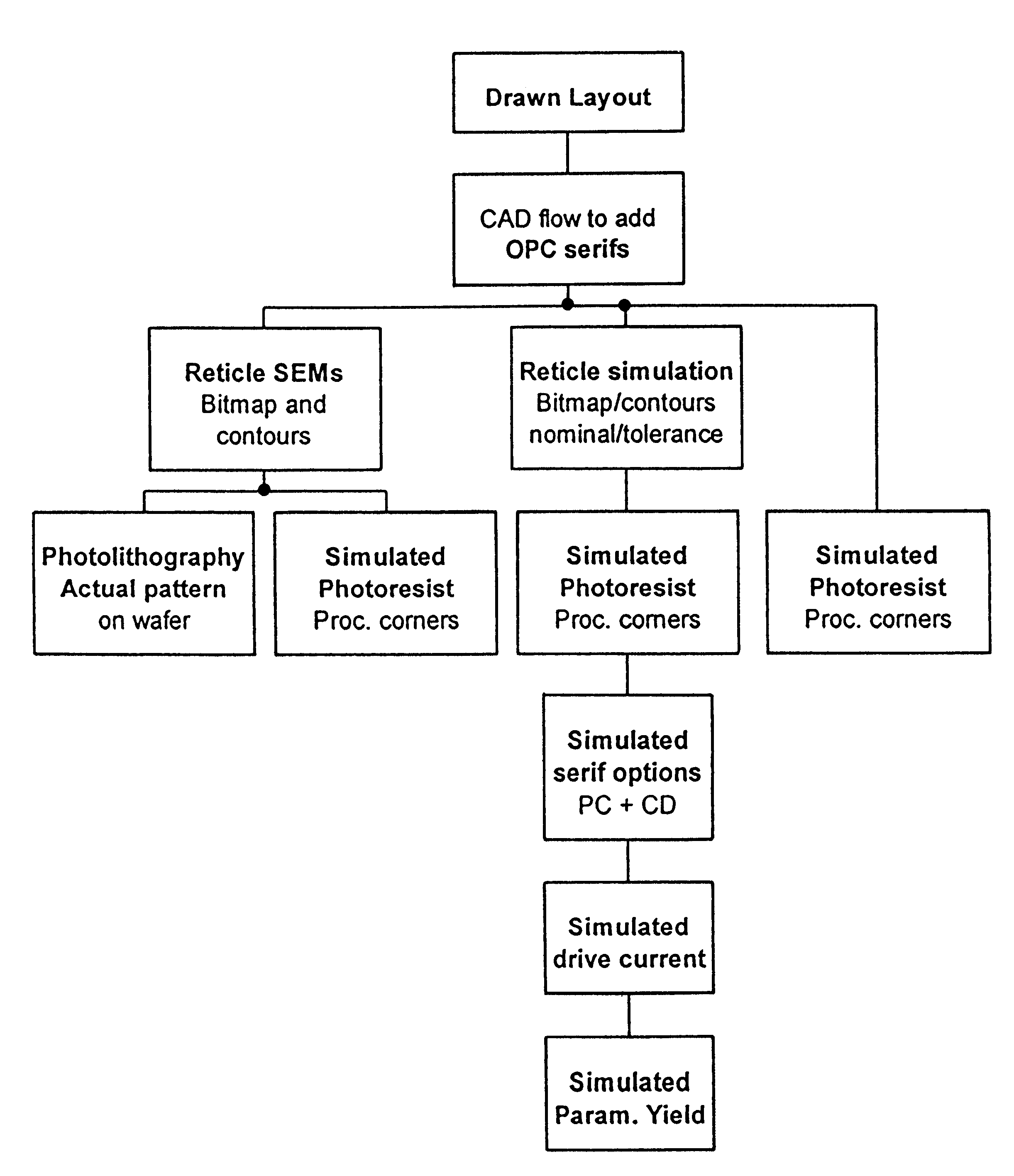
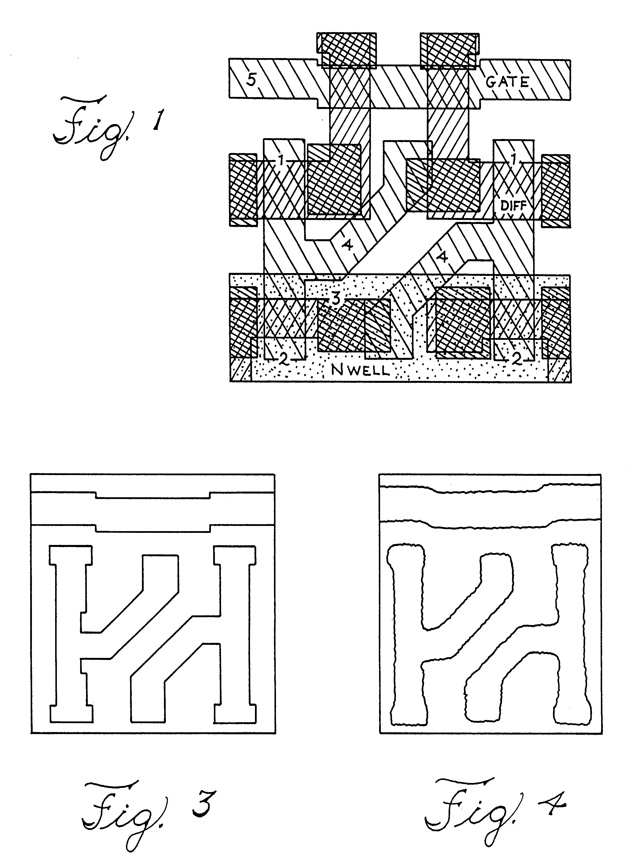
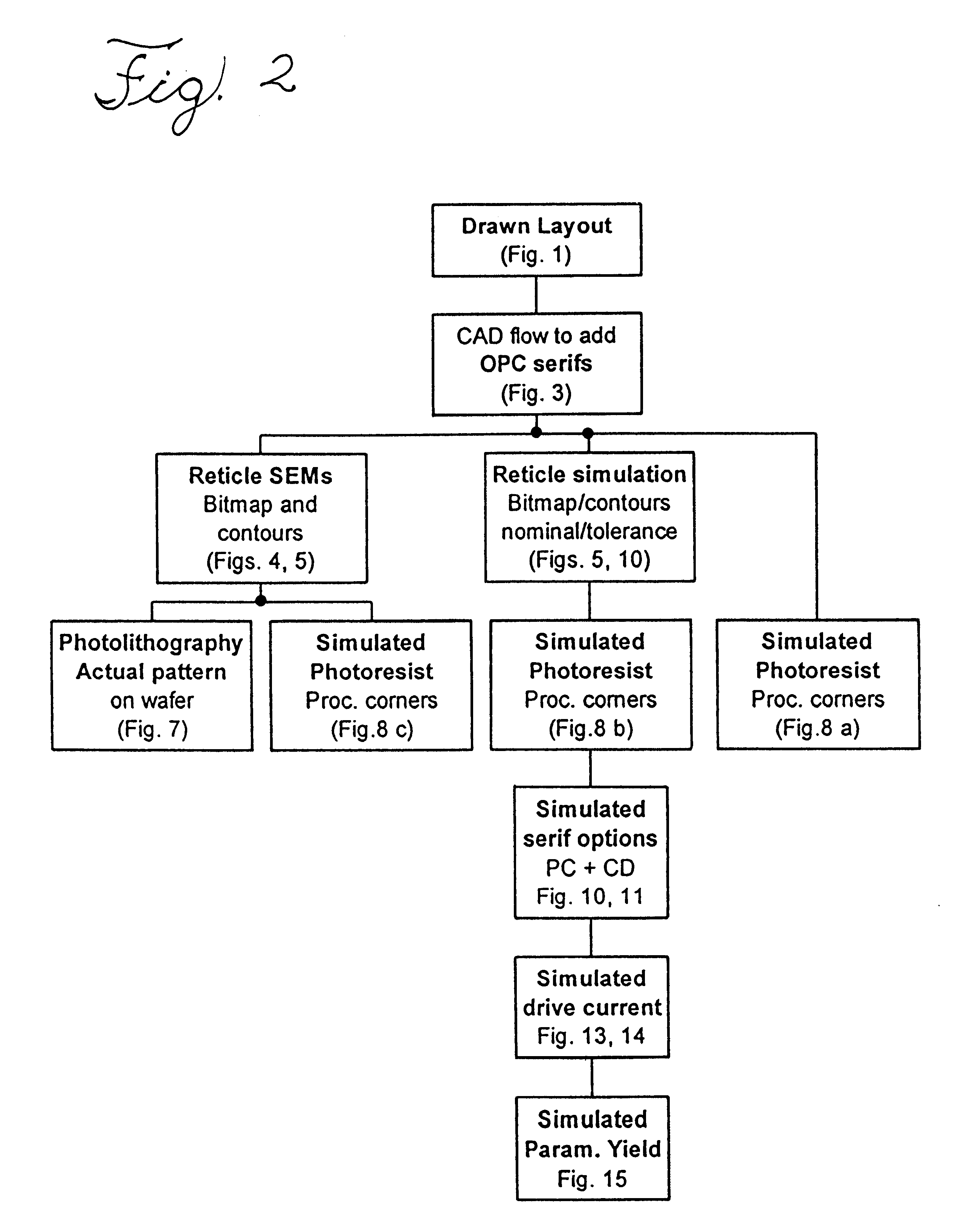
MOSFET parametric yield loss related to the process window of pattern generation was evaluated. In the novel two-step procedure, the shape of MOSFET gates was simulated, by first simulating the mask followed by simulating the photoresist pattern. In the process, the simulation was subsequently calibrated to SEM images of the mask and of the poly pattern on the wafer. Device parameters were then extracted for serif sizes and misalignment corresponding to the mask making and photolithography process windows. We used high density, single wordline six transistor SRAM cell for 0.16 .mu.m technology with complex OPC based mostly on hammerhead serifs. All optical simulations were done using PROLITH2 software from FINLE, and device / yield simulations on SEQUOIA DEVICE DESIGNER (SEQUOIA DEVICE DESIGNER User's Guide, SEQUOIA DESIGN SYSTEMS, 1999).

SRAM Cell

FIG. 1 shows the key layers of the single wordline 6T SRAM cell. While its area of 2.3 .mu.m.sup.2 should be considered as small for the set...

example 2

Line-end registration is an important criterion for pattern fidelity since excessive line-end shortening can cause MOSFET failures, as illustrated in FIG. 17. Line-end reduction of poly over active can lead to transistor short channel effects (threshold voltage variations, low punch through, and high leakage). A distribution of line-end placement errors extracted for a test chip (containing line patterns drawn at 0.25 .mu.m design rules in various configurations and pitches) is shown in FIG. 18, left. Significant shortening of lines up to 130 nm due to optical proximity effects is clearly visible. If uncorrected, they would lead to catastrophic failures of the type indicated in FIG. 17 (i.e. short-channel effects and possibly shorts).

In order to prevent line-end shortening, full-chip automated OPC was applied to the test chip. By adding hammerhead serifs to the ends of poly lines, it was possible to dramatically reduce both the mean value and the variation of poly line end reduction...


PUM


Abstract

A method for determining device yield of a semiconductor device design, includes determining statistics of at least one MOSFET parameter from a gate pattern, and calculating device yield from the at least one MOSFET parameter. The method provides a direct simulation link from device layout to device performance.

Description

The present invention relates to an integrated scheme for predicting yield of semiconductor devices.Within-chip variability of critical features such as polycrystalline silicon (poly) lines due to limitations of manufacturing processes is a major cause of device variability and product yield loss in semiconductor devices. A significant fraction of this variability is a deterministic function of local layout patterns and properties of the manufacturing processes (lithography, etch, etc.). In particular, optical proximity effects on the poly layer can degrade transistor parameters or even lead to catastrophic failures, such as shorts or opens. Gate length variability is the main source of circuit-level variation and a major performance and yield limiter. Sensitivity of transistor performance to gate critical dimension (CD) is a strong function of transistor architecture and, thus, the front-end manufacturing process.Reducing circuit-level variability can be achieved at two levels:(a) ...

Claims


Application Information

Patent Timeline
Patent Type & Authority Patents(United States)
IPC IPC(8): H01L21/66
CPCH01L22/20
Inventor BALASINSKI, ARTURPACK, ROBERT C.AXELRAD, VALERYBOKSHA, VICTOR VLADIMIR
Owner MONTEREY RES LLC
Why Eureka
Try Eureka