Laser irradiation device

a laser irradiation and laser beam technology, applied in non-linear optics, manufacturing tools, instruments, etc., can solve the problems of inconvenient crystallization of semiconductor films, interference of laser beams, and inability to crystallize fifth harmonics

Inactive Publication Date: 2003-05-13
SEMICON ENERGY LAB CO LTD
View PDF18 Cites 77 Cited by
  • Summary
  • Abstract
  • Description
  • Claims
  • Application Information

AI Technical Summary

Problems solved by technology

This is because when the divided laser beams were again converged on one region, the divided laser beams interfered with each other.
The maximum power of the fifth harmonic is lower than the above maximum power and hence the fifth harmonic is not suitable for crystallizing the semiconductor film.

Method used


Image

  • Laser irradiation device
  • Laser irradiation device
  • Laser irradiation device

Examples


embodiment 1

[Embodiment 1]

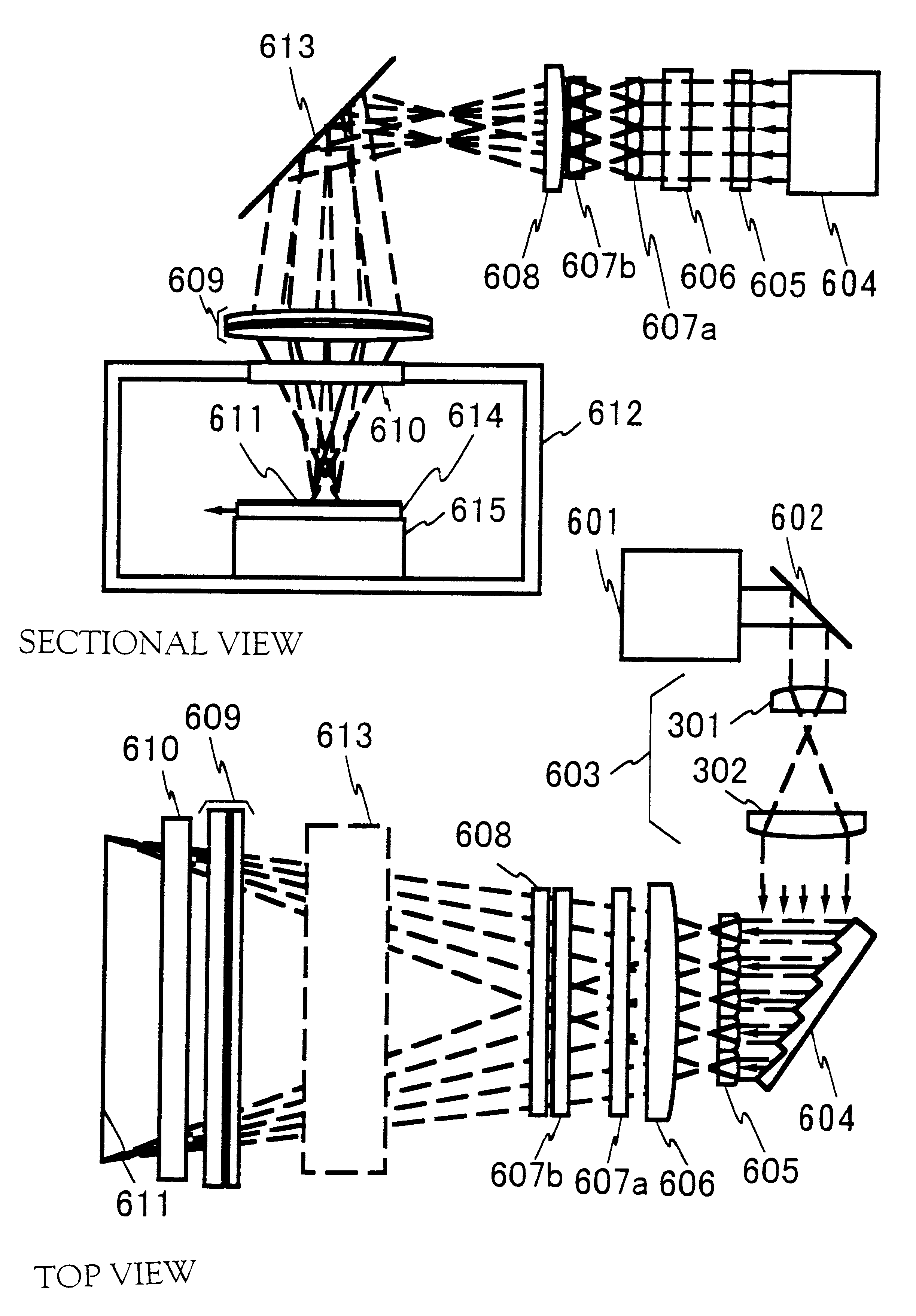
In the present embodiment, an example will be described in which a polycrystalline silicon film is irradiated with a laser beam. The laser irradiation device described in the above preferred embodiment is used as a laser irradiation device for the present embodiment mode.

A Corning glass 1737 having a thickness of 0.7 mm is used as a substrate. The substrate has sufficient durability if it is used under 600.degree. C. An SiO.sub.2 film is formed in 200 nm on one surface of the substrate by a plasma CVD method. Further, an a-Si film is formed in 55 nm on the SiO.sub.2 film. Any other film forming method, for example, a sputtering method may be used.

Next, the above-mentioned a-Si film is crystallized by the method disclosed in Japanese Patent Laid-Open No. 7-130652. The method will be described briefly in the following. The above a-Si film is coated with a nickel acetate water solution having a concentration of 10 ppm and then is heated in a nitrogen atmosphere at 550.deg...

embodiment 2

[Embodiment 2]

In the present embodiment, an example will be described in which the second harmonic of a YAG laser is used as a laser oscillator. The advantage of using the second harmonic resides in that an optical lens resists being degraded by the second harmonic. Also, since the second harmonic has a lower reflectance to the a-Si film than the third harmonic or the fourth harmonic, the energy efficiency obtained when the second harmonic is used is slightly lower than the energy efficiency obtained when the third harmonic or the fourth harmonic is used. The maximum pulse energy now in existence is 1400 mJ / pulse. This is two times the third harmonic and hence it is recommended that the elongated linear laser beam of the second harmonic be used for crystallizing the a-Si film formed on a substrate having a large area.

It is recommended that the same laser irradiation device and method as those described in the preferred embodiment of the present invention be used as the device and me...

embodiment 3

[Embodiment 3]

In the present embodiment, an example will be described in which the fourth harmonic of a YAG laser is used as a laser oscillator. The advantage of using the fourth harmonic resides in that the absorption coefficient of the fourth harmonic to a silicon film is very high.

It is recommended that the same laser irradiation device and method as those described in the preferred embodiment of the present invention be used as the device and method for transforming the fourth harmonic into a linear laser beam and applying it to semiconductor film. However, since the fourth harmonic is different in a wavelength from the third harmonic, it is necessary to change the focal point. In the case of the present embodiment, it is recommended that the distance between the quartz window 610 and the irradiate surface 611 be changed to 126 mm. The coating of the lens is adapted to the wavelength (266 nm) of the fourth harmonic of the YAG laser.

The embodiment 3 can be combined with the embod...


PUM

PropertyMeasurementUnit
lengthaaaaaaaaaa
transmittanceaaaaaaaaaa
thicknessaaaaaaaaaa

Abstract

In annealing a non-single crystal silicon film through the use of a linear laser beam emitted by a YAG laser of a light source, it is the object of the present invention to prevent heterogeneity in energy caused by an optical interference produced in the linear laser beam from having an effect on the silicon film. The laser beam is divided by a mirror 604 shaped like steps into laser beams which have an optical path difference larger than the coherence length of the laser beam between them. The divided laser beams are converged on an irradiate surface 611 by the action of a cylindrical lens array 605 and a cylindrical lens 606 to homogenize the energy of the laser beam in the length direction and to determine the length of the linear laser beam. On the other hand, the laser beams divided by a cylindrical lens array 607 are converged on the irradiate surface 611 by a cylindrical lens 608 and a doublet cylindrical lens 609 to homogenize the energy in the width direction of the laser beam and to determine the width of the linear laser beam. Interference fringes parallel to the width direction of the linear laser beam disappears in the linear laser beam by the action of a mirror 604 shaped like steps. If the silicon film is annealed by the linear laser beam while the linear laser beam is being shifted in the width direction of the linear laser beam, the silicon film is remarkably homogenized as compared with a conventional silicon film.

Description

1. Field of the InventionThe present invention relates to a device for manufacturing a semiconductor device having a circuit constituted by a thin film and, or example, to a device for manufacturing an electro-optical device typified by a liquid display device and an electric device having the electro-optical device as a part. In this connection, in the present specification, a semiconductor device designates in general a device capable of functioning by the use of semiconductor characteristics and includes the above electro-optical device and electric device.2. Description of the Related ArtIn recent years, research and development have been widely conducted on the technologies for performing a laser annealing processing to an amorphous semiconductor film or a crystalline semiconductor film (semiconductor film which is not a single crystal but a polycrystal or a micro-crystal), that is, non-single crystal semiconductor film formed on an insulating substrate such as a glass substrat...

Claims


Application Information

Patent Timeline
Patent Type & Authority Patents(United States)
IPC IPC(8): B23K26/06B23K26/067H01L21/02H01L21/20B23K26/073B23K101/40H01L21/268
CPCB23K26/0604B23K26/0608H01L21/2026B23K26/0738B23K26/067H01L21/02592H01L21/02686H01L21/02488H01L21/02422H01L21/02678H01L21/02532H01L21/0242H01L21/02691H01L21/02675
Inventor TANAKA, KOICHIRO
Owner SEMICON ENERGY LAB CO LTD
Why Eureka
Try Eureka